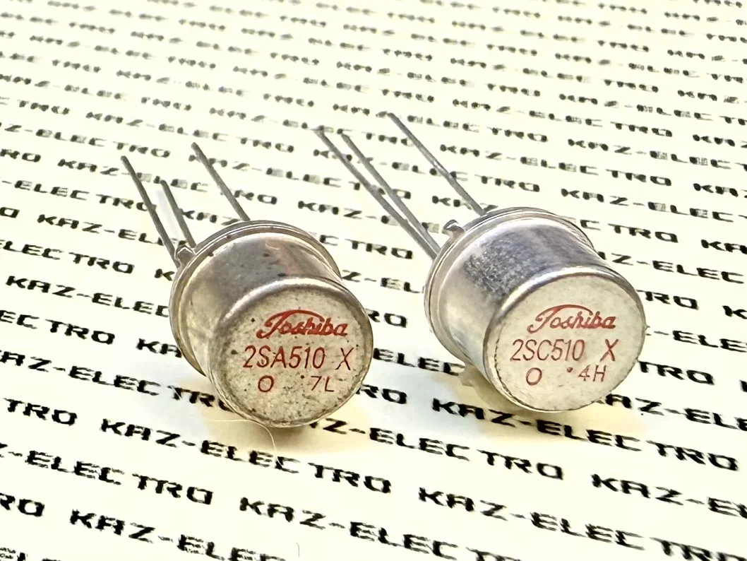
2SA493 / 2SC1000
2SA493G / 2SC1000G
2SA493GTM / 2SC1000GTM
2SC1000TM
Executive Summary
The 2SA493/2SC1000 is Toshiba’s first 50V low-noise complementary pair, released in the early 1970s.
Conceived with Hi-Fi audio in mind, this pair satisfied all three essentials for solid-state amplifier design: high breakdown voltage, low noise, and complementary symmetry. At a time when low-noise transistors in the 20–30V class were the norm, the arrival of a 50V-class option carried real weight — and made an impact in an era when vacuum tube amplifiers still dominated.
This article traces the roughly 20-year journey of the 2SA493/2SC1000, from development to discontinuation, through the lens of both the technical and market forces of the period.
This article covers considerable ground and is fairly extensive. A table of contents follows; readers are welcome to jump directly to the sections of greatest interest.
Key Points
Databook Reference (Chapters 3–6)
- Datasheet information for the Original, G, and GTM types
- Positioning and product history of each variant
Technology History and Development Background (Chapters 7–11)
- The Four Technical Hurdles of low-noise PNP development, and how they were overcome
- A development race timeline spanning 6 manufacturers and approximately 40 competing devices
- Reading manufacturing process history through markings and appearance
Characteristic Comparison and Verification (Chapter 11)
- hFE–IC curve comparison across family members
- Measured data from a custom-built test instrument
- Die identity analysis between early and late production
Compatibility Selection Guide (Chapter 13)
- Practical replacement information based on verified results
- Comprehensive coverage of compatible alternatives recommended by Toshiba, Sony, and CQ Publishing
See the table of contents to jump directly to any chapter.
1. Overview
1.1 Product Position
The 2SA493/2SC1000 is the direct ancestor of the 2SA970/2SC2240 — the pair that would go on to reign as Toshiba’s definitive low-noise audio transistor for more than three decades.
This complementary pair debuted in the early 1970s in Toshiba’s proprietary TO-98 package. Within a decade, the family would face a major turning point. Manufacturing methods for small-signal transistors were overhauled across the industry, and a wave of rationalization brought a transition to the TO-92 package.
Other products that had debuted in TO-98 were similarly consolidated and restructured. The rationalization wave swept through this family as well, and the torch for consumer applications passed to the next generation.
The 2SA493G/2SC1000G, developed as a high-reliability grade for industrial equipment, was a different story. Backed by long-term maintenance demand, it survived the TO-92 transition with supply intact. Its part numbers were revised to 2SA493GTM/2SC1000GTM alongside the package change, and production continued into the early 1990s.
This history gave the family a product life cycle spanning roughly 20 years.
1.2 Application Examples
When the 2SA493/2SC1000 debuted, demand for silicon transistors was climbing sharply. The resin-encapsulated TO-98 product line was Toshiba’s answer to that demand. The 2SA493 in particular drew attention as a pioneer among low-noise PNP silicon transistors — achieving a breakdown voltage of 50V and a maximum hFE of 400, both advanced figures for the time.
That said, the TO-98 was a transitional form — not yet the fully automated mass-production method that would follow. Like germanium transistors before it, the package still required substantial manual labor at multiple stages. In terms of productivity and cost, it carried inherent limitations. Even so, the pair’s strong specifications earned it adoption across a wide range of products, audio equipment chief among them.
- Audio amplifiers: In the ONKYO Model 732 (1972) and Model A-7022 (1974), the pair was used in RIAA equalizer and tone control circuits where low noise was essential. The DENON PMA-850 (1977) employed it in the main amplifier’s protection circuit as well — a testament to the versatility that its high hFE enabled.
- Recording and playback equipment: Open-reel tape decks such as the TEAC A-7300RX used it in playback amplifiers (head amplifiers), where low noise was a priority.
- Musical instrument effects: Roland’s AF-60 “Bee Gee Fuzz” (c. 1975) combined an early TA7504M op-amp with the 2SC1000. The AD-50 “Double Beat” wah/fuzz combination unit (1973) used it in the amplification stage. In later BOSS compact effects (OD-1, DS-1, CE-2, and others), the successor 2SC2240 would become the standard choice. Tracing the lineage of effects circuit design leads back to the 2SC1000 of the 1970s.
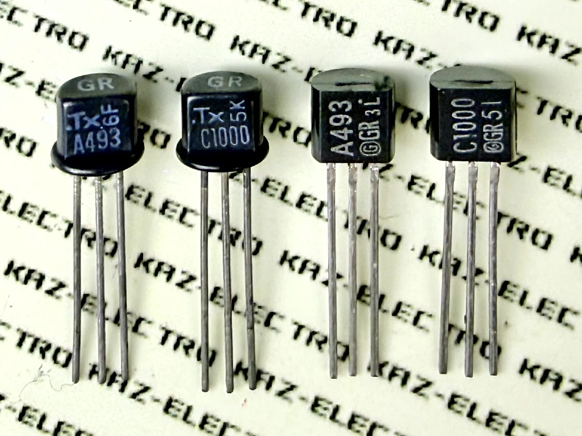
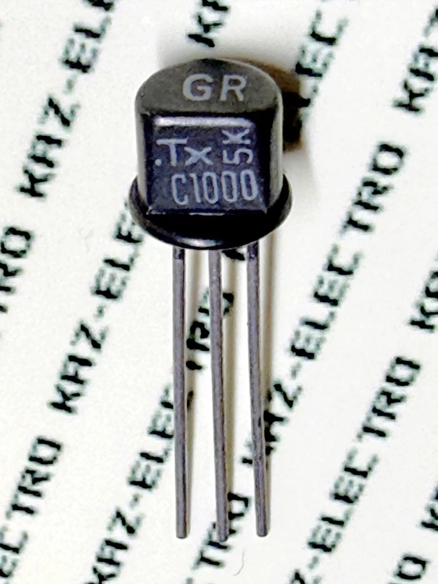
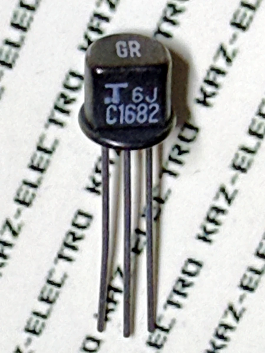
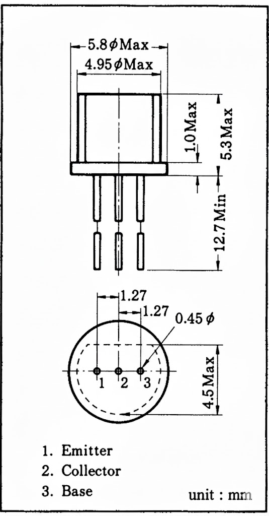
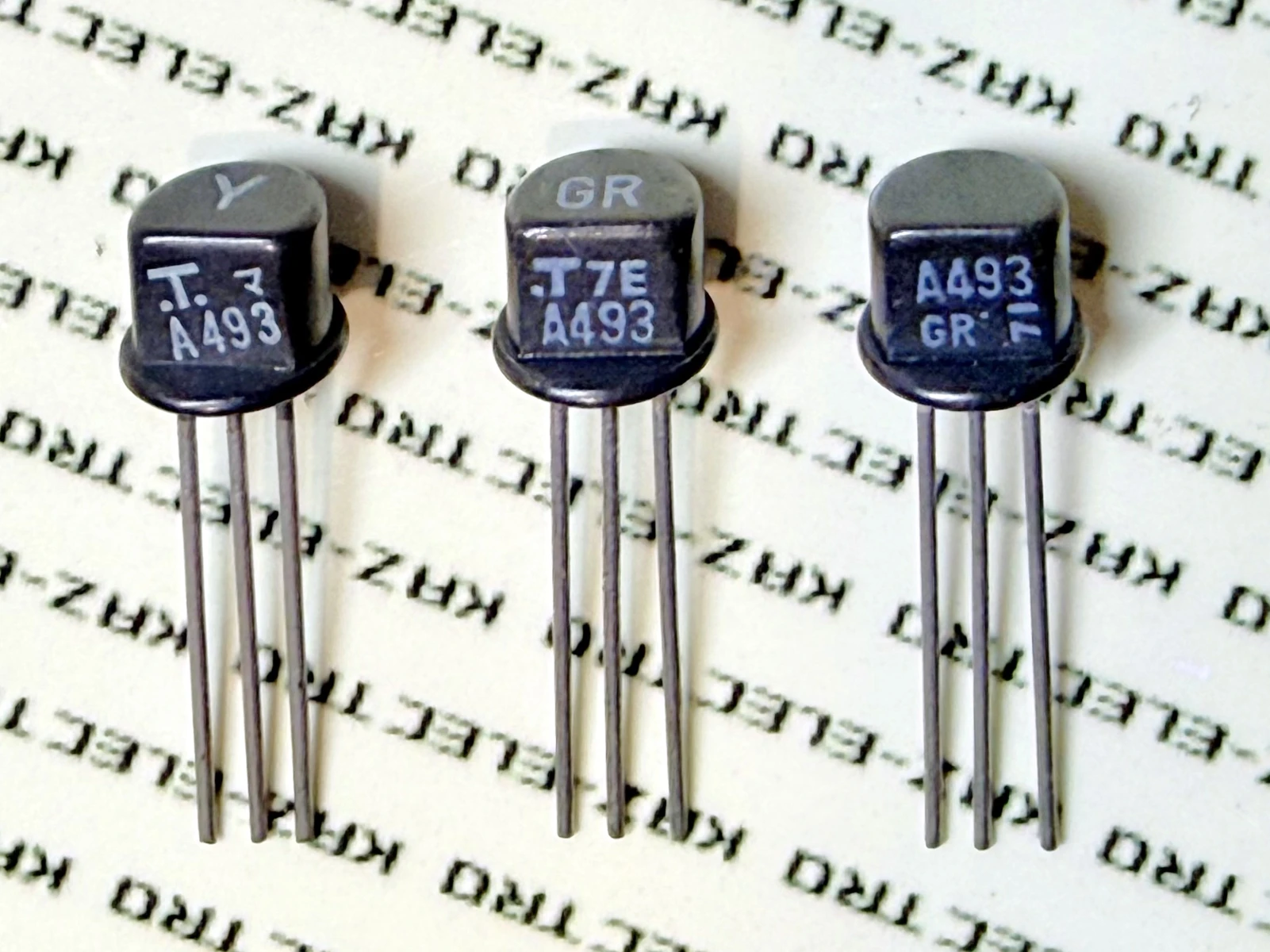
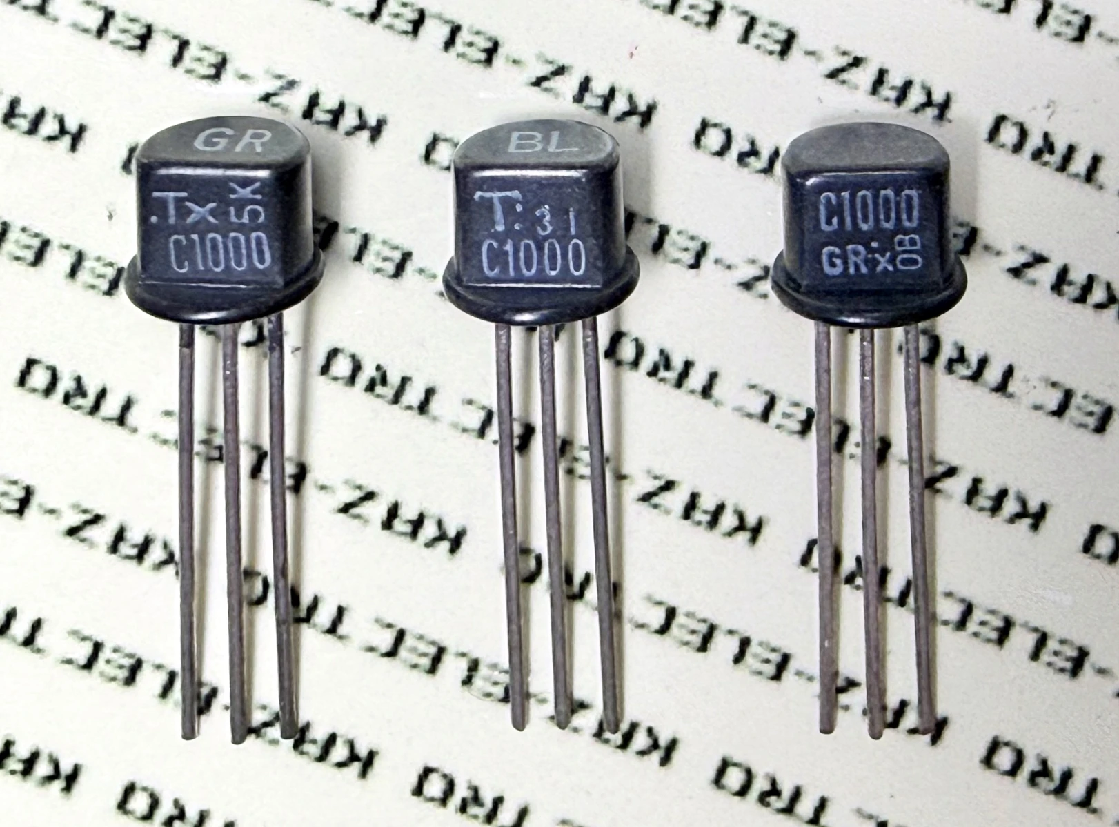
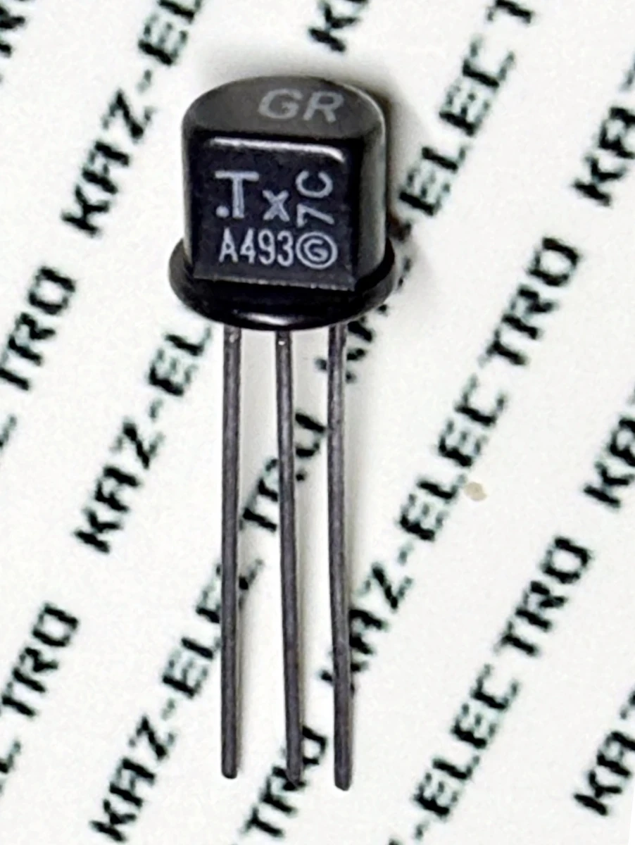
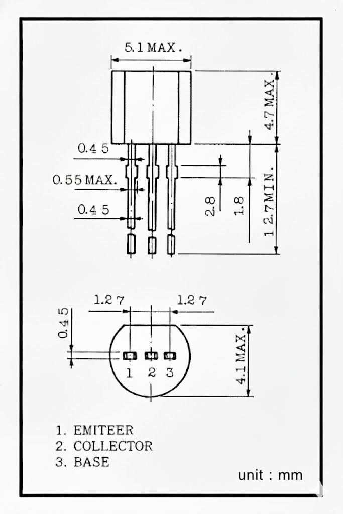
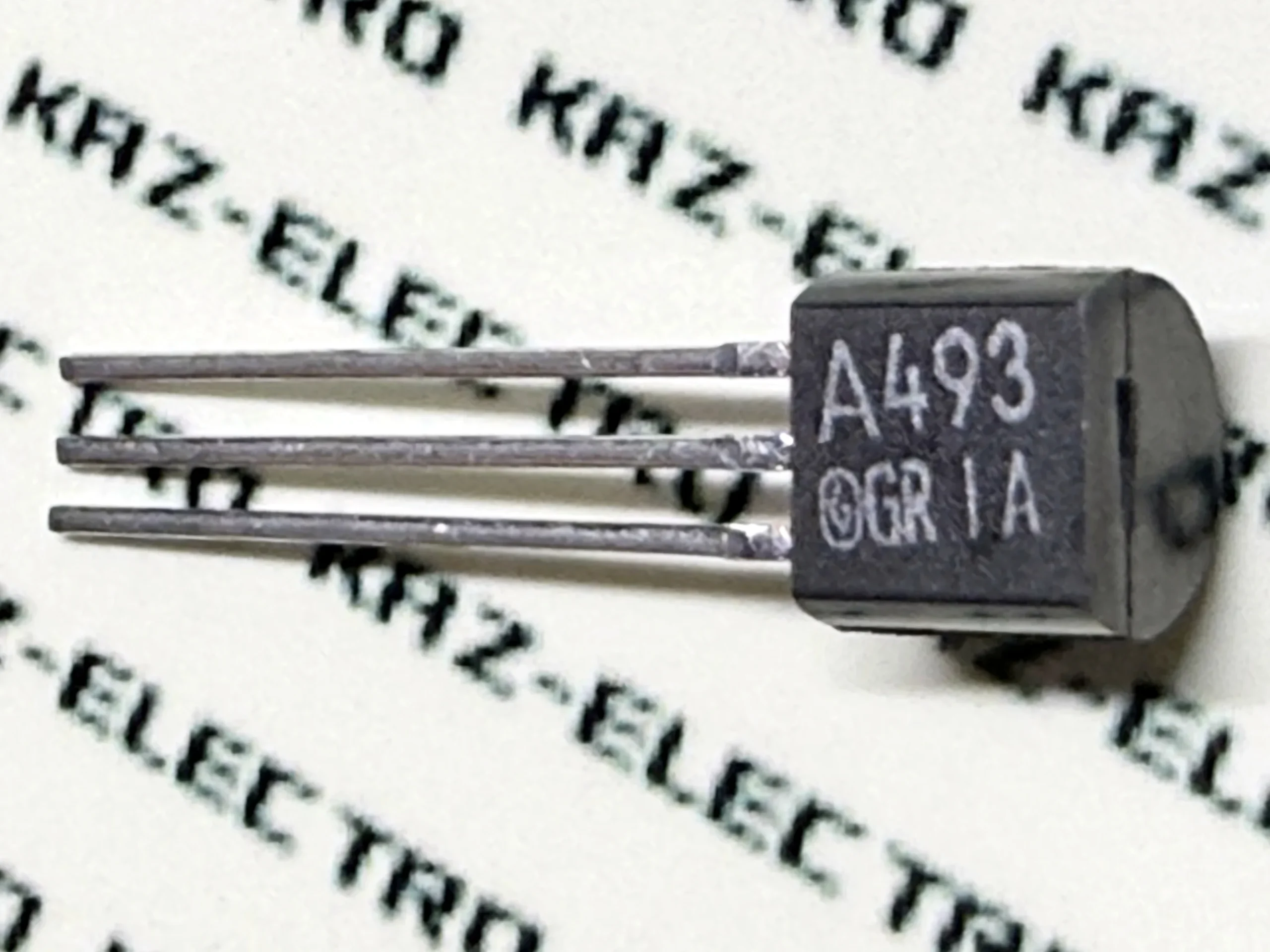
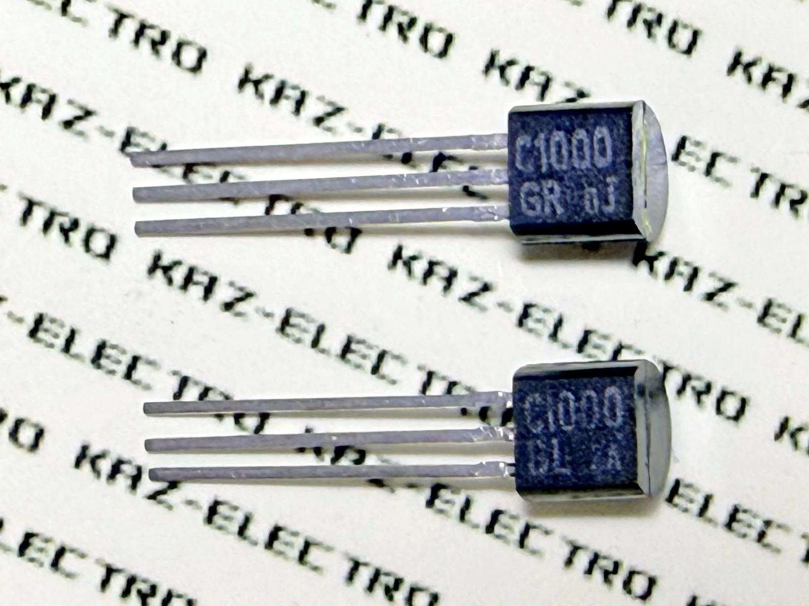
1.3 Visual Identification
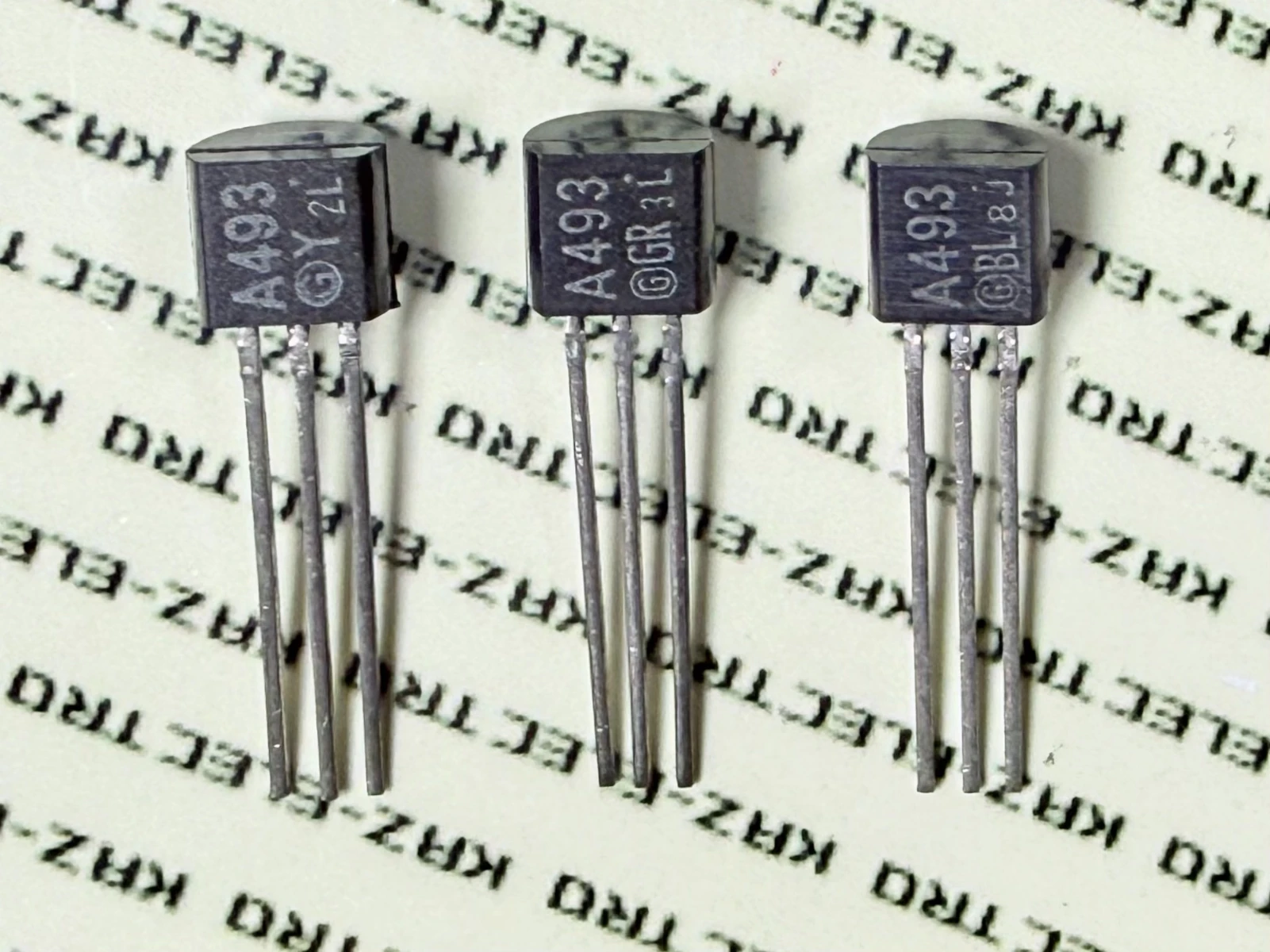
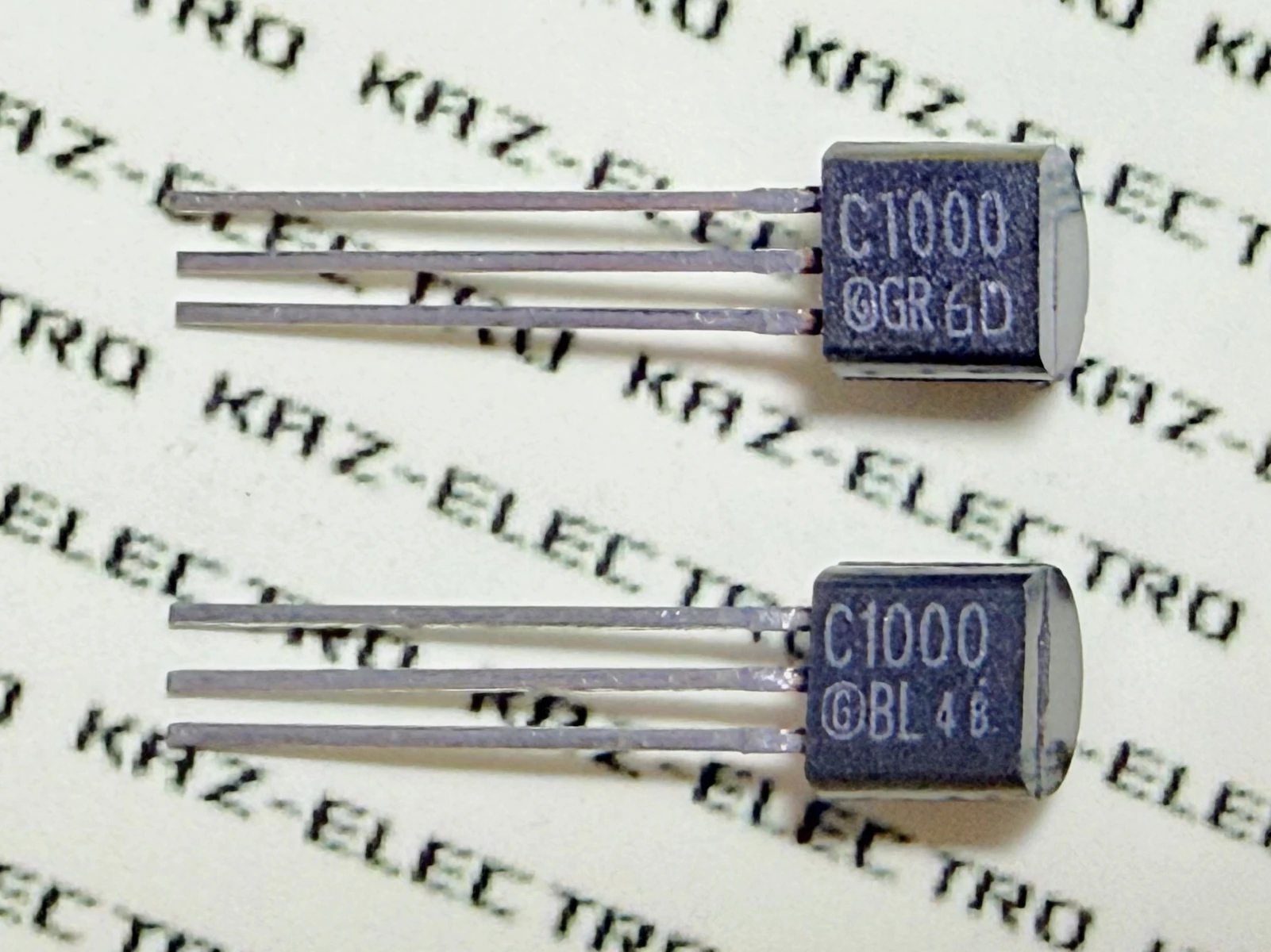
The most distinctive feature of Toshiba’s TO-98 package products is the hFE rank marking applied to the top surface. This marking changed with time, making it possible to estimate the manufacturing period from the device’s appearance alone.
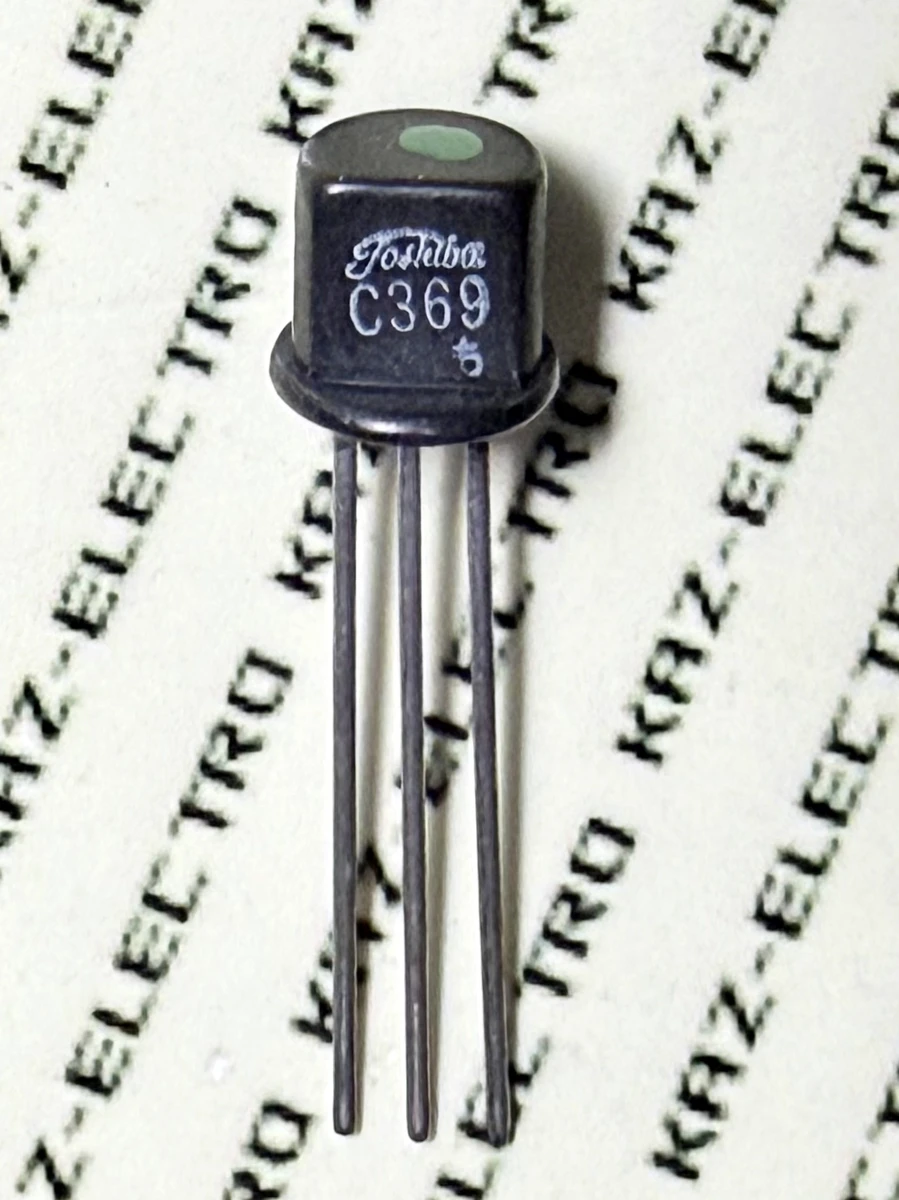
Early period: hand-applied color dots (e.g., 2SC369-GR / mid-1960s)
Middle period: standard-font printing (e.g., 2SC1000-GR / late 1960s–mid 1970s)
Late period: narrow-font printing (e.g., 2SC1682-GR / mid-1970s)
Final period: top marking discontinued, moved to part number face (e.g., 2SC1000-GR / late 1970s–1981)
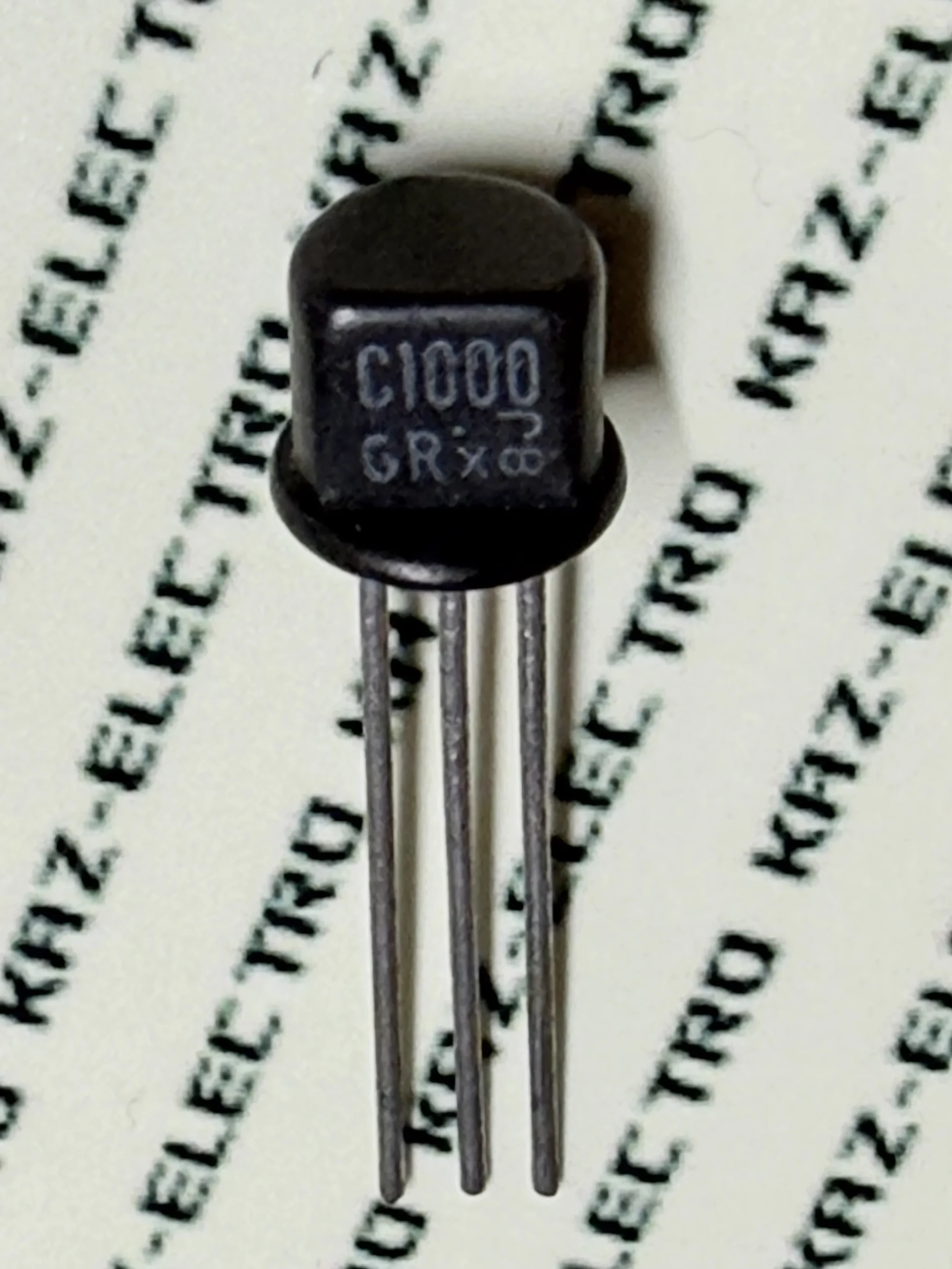
Members of Toshiba’s TO-98 low-noise series. The 2SC369 of the earlier generation, the 2SC1682 of the later generation, and the 2SC1000 itself — each changed its appearance over time. Even a single photograph conveys the differences between generations.
A glance at the top surface reveals something about the era the device passed through. For a collector who sees these not merely as components but as fragments of history, this is one of the quiet pleasures. The technical background behind these changes is examined in Chapter 10, “Process Rationalization.”
1.4 A Memorable Part Number
The round-number designation “2SC1000” made it exceptionally easy to remember — for engineers and hobbyists alike — and that no doubt contributed to its popularity. As a byword for high-hFE transistors, the name appeared not only in audio circles but frequently in the construction articles of radio-building magazines and amateur radio publications of the time.
Popular parts, once discontinued, vanish from the market quickly. As of 2025, tracking down the original type has become extremely difficult. Even after more than forty years of searching, the author has managed to secure only a small number of pieces.
There was a long stretch of time when walking into a shop and asking for a “2SC1000” would, nine times out of ten, get you the successor — a small but familiar disappointment.
The successor in question is the GTM type — the final evolution of this family. That a part originally rated as an industrial-grade device had penetrated deep into general hobby electronics shops says something about the breadth of Toshiba’s domestic supply network at the time.
2. Family Overview
2.1 The Complex Evolution of Databook Content: 1960s–70s
The 1960s and 70s were a period of rapid advance in semiconductor technology. The 2SA493/2SC1000, which appeared during this era, evolved year by year — its maximum ratings, specifications, and characteristics shifting in ways that can be difficult to untangle. This chapter draws on devices in the author’s collection alongside databooks and manufacturer materials from successive years, with the aim of mapping this evolution in full.
2.2 Timeline
The 2SA493/2SC1000 family comprises four variants, shown below.
| Production Period | Family | Part Numbers | Package | Application | Notes |
|---|---|---|---|---|---|
| c. 1971–1981 | Original type | 2SA493 / 2SC1000 | TO-98 | Consumer | Original |
| G-type | 2SA493G / 2SC1000G | TO-98 | Telecom/Industrial | High-reliability grade | |
| c. 1978–1991 | GTM-type | 2SA493GTM / 2SC1000GTM | TO-92 | Telecom/Industrial | TO-92 transition |
| c. 1978–1984 | TM-type | 2SC1000TM | TO-92 | NRND | Not listed in databooks |
2.3 hFE Rank Overview by Family
The 1960s and 70s were still deeply marked by vacuum tube design conventions. Discrete transistor circuits were the norm, and designers had no choice but to account carefully for individual device parameters.
The hFE figure, in particular, was subject to wide variation — a consequence of the manufacturing challenges of the time — and knowing it accurately was a basic requirement of circuit design.
During the era of germanium transistors, it was not unusual for manufacturers to assign different part numbers to devices that differed only in hFE range. That practice carried into the silicon age, and hFE scatter continued to frustrate both manufacturers and their customers. In response, semiconductor makers began adopting the concept of hFE rank classification.
In practice, this meant testing each device’s hFE, sorting devices into ranges, and appending a manufacturer-specific suffix to the part number — a convenience that gave users a reliable way to specify what they needed.
Toshiba’s notation used “O,” “Y,” “GR,” and “BL.” These letters trace back to the earliest days of the classification system, when color dots were applied by hand. O stands for Orange, Y for Yellow, GR for Green, and BL for Blue.
In amateur construction articles of the time, selecting a rank to suit the application was taken for granted. A circuit prone to high-frequency oscillation might call for a low-hFE grade; one demanding gain or high input impedance would call for a high-hFE grade. That kind of design thinking was commonplace.
Equipment manufacturers operated similarly. Some designed circuits tolerant of any rank; others specified ranks precisely. Large-volume customers could sometimes obtain specially sorted devices. The author plans to return to this topic in a future article.
hFE Rank Table
The hFE rank classification scheme changed across databook editions.
hFE Rank Legend
O: 70–140 / Y: 120–240 / GR: 200–400 / BL: 350–700
| Databook Year |
Original type | G-type | GTM-type | |||
|---|---|---|---|---|---|---|
| 2SA493 | 2SC1000 | 2SA493G | 2SC1000G | 2SA493GTM | 2SC1000GTM | |
| 1971 (Handy Book) |
O / Y / GR | Y / GR / BL Y rank present |
— | — | — | — |
| 1973 | O / Y / GR | GR / BL Y rank dropped |
Y / GR | GR / BL | — | — |
| 1975 | Y / GR O rank dropped |
GR / BL | Y / GR | GR / BL | — | — |
| 1977 | NRND | GR / BL | GR / BL BL added |
GR / BL | Y / GR / BL ?* | GR / BL ?* |
| 1980 | NRND | NRND | NRND | NRND | Y / GR BL dropped (rank regression) |
GR / BL |
Source: TOSHIBA Semiconductor Handbook 1973/1975; TOSHIBA Semiconductor Databook 1977/1980
* Details of the 2SA493GTM/2SC1000GTM as produced between 1977 and 1979 remain unresolved. The first official datasheet for these types does not appear until the 1980 databook edition.
2.4 Family Specification Summary
A consolidated overview of the key specifications across all four variants. Refer to the individual chapters for details.
| Parameter | Original type | G-type | GTM-type | TM-type |
|---|---|---|---|---|
| Package | TO-98 | TO-98 | TO-92 | TO-92 |
| Application | Consumer | Telecom/Industrial | Telecom/Industrial | Consumer (NRND) |
| Vcbo (V) | −50 / 50–55 | −50 / 55 | −50 / 60 | (not disclosed) |
| Vceo (V) | −50 / 50 | −50 / 50 | −50 / 50 | (not disclosed) |
| Ic (mA) | −50 / 100 | −50 / 100 | −150 / 150 | (not disclosed) |
| Pc (W) | 0.2 / 0.2 | 0.2 / 0.2 | 0.4 / 0.4 | (not disclosed) |
| fT (MHz) | — / 80 | 80 / 80 | 80 / 80 | (not disclosed) |
| Cob (pF) | — / 6 | 6 / 6 | 6 / 6 | (not disclosed) |
| NF (dB) | 2 / 3 | 2 / 2 | 2 / 2 | (not disclosed) |
| Details | → Ch. 3 | → Ch. 4 | → Ch. 5 | → Ch. 6 |
Values are listed in PNP / NPN order. NF maximum values: PNP at f = 120 Hz; NPN at f = 100 Hz; Rg = 10 kΩ; Ic = 0.1 mA. TM-type specifications are undisclosed, as this variant does not appear in any known databook.
[Chapter 2 Summary] The 2SA493/2SC1000 family underwent a complex evolution across the 1970s and 80s — from consumer-grade (Original) to telecom/industrial-grade (G), and ultimately to the TO-92 transition (GTM/TM). Databook content shifted with each edition, which means that determining the actual specifications and characteristics of a given device requires cross-referencing part number, appearance, and manufacturing lot. That is one of the main reasons this site devotes so much space to documenting this family in depth.
→ Subsequent chapters cover the detailed specifications of each family member individually.
3. 2SA493/2SC1000 (Original Type)
Chapter contents: Specifications, characteristics, and product history of the original version, with a comparative analysis against the successor devices 2SA970/2SC2240.
The first generation of the 2SA493/2SC1000 family was introduced in Toshiba’s proprietary TO-98 package. Its distinctive silhouette has earned it the affectionate nickname “top-hat package” among many enthusiasts.
3.1 Characteristics
2SA493
- Low-frequency, low-noise amplification
- High breakdown voltage: VCEO = −50 V
- Low noise: NF = 2 dB (max) (f = 120 Hz, Rg = 10 kΩ)
2SC1000
- Low-frequency, low-noise amplification
- High breakdown voltage: VCEO = 50 V
- Low noise: NF = 3 dB (max) (f = 100 Hz, Rg = 10 kΩ)
- High current gain: hFE = 200–700
3.2 Maximum Ratings and Electrical Characteristics
| Parameter | 2SA493 (1975) | 2SA493 (1973) | 2SC1000 (1975/1977) | 2SC1000 (1973) |
|---|---|---|---|---|
| Process | SiP (PCT) | SiEP | SiP (PCT) | SiEP |
| Vcbo (V) | −50 | −50 | 50 | 55 |
| Vceo (V) | −50 | −50 | 50 | 50 |
| Vebo (V) | −5 | −5 | 5 | 5 |
| Ic (A) | −0.05 | −0.05 | 0.1 | 0.1 |
| Pc (W)*Ta = 25°C | 0.2 | 0.2 | 0.2 | 0.2 |
| hFE*|Vce| = 6 V, |Ic| = 2 mA | Y: 120–240 GR: 200–400 |
O: 70–140 Y: 120–240 GR: 200–400 |
GR: 200–400 BL: 350–700 |
GR: 200–400 BL: 350–700 |
| fT (MHz)*Vce = 6 V, Ic = 1 mA | — | — | Typ. 80 | Typ. 80 |
| Cob (pF)*Vcb = 6 V | — | — | Typ. 6 Max. 10 |
Typ. 6 Max. 10 |
| NF (dB)*Ic = 0.1 mA, Rg = 10 kΩ | Max. 10 (10 Hz) Max. 2 (120 Hz) |
Max. 10 (10 Hz) Max. 2 (120 Hz) |
Max. 10 (10 Hz) Max. 3 (100 Hz) |
Max. 10 (10 Hz) Max. 3 (100 Hz) |
Source: TOSHIBA Semiconductor Handbook 1973/1975; TOSHIBA Semiconductor Databook 1977/1980
SiP: Silicon Planar; SiP (PCT): Silicon Planar (PCT process); SiEP: Silicon Epitaxial Planar
3.3 hFE Rank Configuration
| Part Number | Rank Configuration | Notes |
|---|---|---|
| 2SA493 | O / Y / GR → Y / GR | O rank discontinued from 1975 onward |
| 2SC1000 | GR / BL | No change |
3.4 Product History
| Event | 2SA493 | 2SC1000 |
|---|---|---|
| Introduction | c. 1971 | c. 1971 |
| NRND designated | 1976 | 1979 |
| Discontinued | c. 1981 | c. 1981 |
| Toshiba recommended replacement | 2SA842 2SA970 |
2SC732TM 2SC2240 |
Source: TOSHIBA Semiconductor Databook 1977/1980/1983
For a full survey of compatible and replacement devices, see also Chapter 13, “Compatibility Selection Guide.”
3.5 Discussion
On hFE Ranks
One detail about the 2SA493 deserves mention. For a brief period immediately after its introduction, an O-rank variant — hFE 70–140 — appeared in the documentation.
Low-noise transistors deliver their greatest value in small-signal amplification circuits where achieving an adequate S/N ratio is the overriding requirement. In that context, a higher hFE is generally desirable — the more gain the device can provide, the better.
By the mid-1970s, Toshiba’s BL rank reached an upper hFE limit of 700, while competing and successor devices were beginning to appear with maximum hFE values of 800 to 1,200. Against that backdrop, the O-rank hFE of 70–140 appears comparatively low.
This is most likely one consequence of the technical challenges specific to silicon PNP transistor development. For a detailed discussion, see Section 8.2, “The Four Technical Hurdles of Low-Noise PNP Development.”
Note: The 1972 edition of 『初歩のラジオトランジスタ・ハンドブック』 (Transistor Handbook for Beginners, Seibundo Shinkosha, 1972) lists a V rank for the 2SC1000 — hFE 600–1,200 — alongside the standard GR and BL ranks. This rank never appeared in any official Toshiba databook, and it was in all likelihood discontinued at an early stage due to yield and variation control problems.
Note: Toshiba showed a tendency to introduce high-hFE ranks on a temporary basis. See also: Section 12.4.1, “Reading the hFE Rank Transitions,” and Section 6.4.4, “Conclusions.”
On Replacement Devices
The 1977 databook — published shortly after the 2SA493 was designated NRND — lists the 2SA842 as its recommended replacement. With a VCEO of only 40 V, however, this choice looks underspecified. The 2SA841 (a sister device to the 2SA842) with its 60 V rating would appear to be the more appropriate match.
The 2SC1000, still in active production at that point, was given no replacement recommendation.
When the 2SC1000 was itself designated NRND in 1979, Toshiba offered two alternatives: the 2SC732TM, which had no complementary pair, and the then-new 2SC2240. The replacement for the 2SA493 was simultaneously updated to the 2SA970 — the complementary pair for the 2SC2240.
By that point, the 2SA841/2SC1681 and 2SA842/2SC1682 had also been designated NRND, which meant the 2SC168X series reached the end of its life without ever being formally proposed as a replacement for the 2SC1000.
For a detailed comparison of characteristics between the 2SA493/2SC1000 and its successors 2SA970/2SC2240, see Chapter 11, “Verification,” where hFE–IC curves from the databooks are examined in full.
Source: TOSHIBA Semiconductor Handbook 1975 / Databook 1980; CQ Publishing, 『最新トランジスタ互換表』 (Latest Transistor Compatibility Reference) 1970–1982; 『最新トランジスタ規格表』 (Latest Transistor Specification Reference) 1968–1988
[Chapter 3 Summary] Through incremental specification revisions, the 2SA493/2SC1000 established itself as a versatile all-rounder among low-noise transistors. Both types were designated NRND between 1976 and 1979, and production ended around 1981. The 2SA970/2SC2240 stepped into their role as successors.
→ Next chapter: The “Telecom/Industrial Green Series” — the high-reliability grade developed for industrial and communications equipment.
4. 2SA493G/2SC1000G (G-Type)
Chapter contents: Specifications and characteristics of the high-reliability grade for industrial and telecom applications, along with evidence that these devices are sorted from the same die as the original type.
“2SA493G/2SC1000G” is a derivative of the original plain “2SA493/2SC1000,” positioned as the Telecom/Industrial grade variant. The “G” suffix derives from the initial letter of Toshiba’s “Telecom/Industrial Green Series.”
A Note on Terminology
In this article, the term “Telecom/Industrial” is used in accordance with the original Japanese wording found in Toshiba databooks.
In the Japanese semiconductor industry of the 1960s–70s, “Telecom (通信)” did not refer to general consumer communications in the modern sense. It meant infrastructure-class end users: NTT Public Corporation (the predecessor of NTT) and NHK/commercial broadcasters.
While most manufacturers simply labeled their products as “Industrial,” Toshiba chose the more specific “Telecom/Industrial” — the author suspects this may have been a deliberate choice to emphasize that these were high-reliability devices supporting critical infrastructure. Whether Toshiba harbored such intent cannot be confirmed. This archive respects Toshiba’s original terminology and uses it as-is.
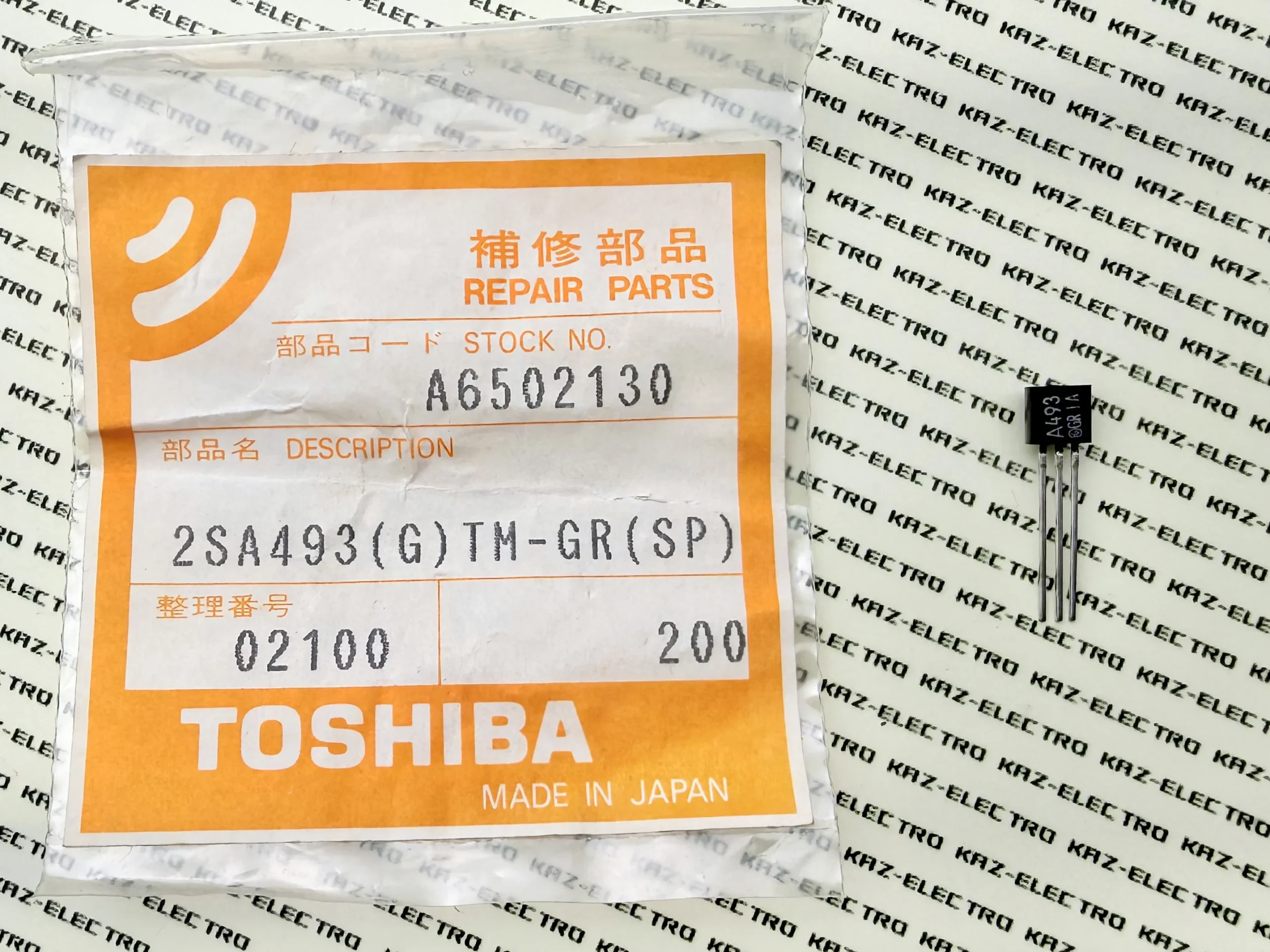
The small “G mark” visible at the end of the part number is the identifying symbol of the Green Series. Regrettably, the 2SC1000G has not yet been obtained for this site.
4.1 Features of the 2SA493G/2SC1000G
2SA493G
- Telecom/Industrial Green Series
- Low-frequency, low-noise amplification
- Complementary pair use with 2SC1000G
- High breakdown voltage: VCEO = −50V
- Low noise: NF = 2dB (max) (f = 120Hz, Rg = 10kΩ)
2SC1000G
- Telecom/Industrial Green Series
- Low-frequency, low-noise amplification
- Complementary pair use with 2SA493G
- High breakdown voltage: VCEO = 50V
- High current gain: hFE = 200–700
- Low noise: NF = 2dB (max) (f = 100Hz, Rg = 10kΩ)
4.2 Maximum Ratings and Electrical Characteristics
As with the standard grade, slight variations can be observed in maximum ratings such as Vcbo depending on production period.
| Parameter | 2SA493G (1977) | 2SA493G (1973) | 2SC1000G (1977) | 2SC1000G (1973) |
|---|---|---|---|---|
| Process | SiP (PCT) | SiEP | SiP (PCT) | SiEP |
| Vcbo (V) | -50 | -50 | 55 | 55 |
| Vceo (V) | -50 | -50 | 50 | 50 |
| Vebo (V) | -5 | -5 | 5 | 5 |
| Ic (A) | -0.05 | -0.05 | 0.1 | 0.1 |
| Pc (W)*Ta=25°C | 0.2 | 0.2 | 0.2 | 0.2 |
| hFE*Vce=6V, Ic=2mA | Y:120-240 GR:200-400 BL:350-700 |
Y:120-240 GR:200-400 |
GR:200-400 BL:350-700 |
GR:200-400 BL:350-700 |
| fT (MHz)*Vce=6V, Ic=1mA | Typ.80 | Typ.80 | Typ.80 | Typ.80 |
| Cob (pF)*Vcb=6V | Typ.6 | Typ.6 | Typ.6 | Typ.6 |
| NF (dB)*Ic=0.1mA, Rg=10kΩ | Max.10 (10Hz) Max.2 (120Hz) |
Max.10 (10Hz) Max.2 (120Hz) |
Max.10 (10Hz) Max.2 (100Hz) |
Max.10 (10Hz) Max.2 (100Hz) |
Source: TOSHIBA Semiconductor Handbook 1973/1975; TOSHIBA Semiconductor Databook 1977/1980/1983/1986
SiP: Silicon Planar; SiP(PCT): Silicon Planar (PCT process); SiEP: Silicon Epitaxial Planar
4.3 hFE Rank Configuration of the 2SA493G/2SC1000G
| Type | Rank Configuration | Notes |
|---|---|---|
| 2SA493G | Y/GR → GR/BL | BL added in 1977 |
| 2SC1000G | GR/BL | No change |
4.4 Product History
| Item | 2SA493G | 2SC1000G |
|---|---|---|
| Introduction | c. 1971 | c. 1971 |
| NRND designated | 1979 | 1979 |
| Discontinued | c. 1981 | c. 1981 |
| Toshiba recommended replacement | 2SA493GTM 2SA970 |
2SC1000GTM 2SC2240 |
Source: TOSHIBA Semiconductor Handbook 1973/1975; TOSHIBA Semiconductor Databook 1977/1980/1983; Transistor Compatibility Reference (『最新トランジスタ互換表』, CQ Publishing, 1970–1982)
For a summary of compatible replacements, refer to Chapter 13 “Compatible Device Selection Guide.”
4.5 Discussion
Details of the “Green Series”
According to the datebook, “Toshiba Telecom/Industrial transistors” are products designed and manufactured for “communications, measurement, medical electronics, and control equipment” — applications requiring a higher degree of operational reliability than consumer entertainment equipment.
The same datebook contains the following passage:
“Should these devices fail, the consequences could include enormous economic losses, serious social disruption, and in some cases threats to human life. It is strongly required that they perform as intended even under harsh environmental conditions including vibration, shock, temperature extremes, and humidity.”
Within this category, two tiers exist: “Telecom/Industrial Exclusive Transistors,” manufactured under the strictest MIL-equivalent controls; and “Green Series transistors,” which have undergone comparable but slightly less stringent testing. The latter are defined as follows:
“Products whose characteristics have been stabilized through temperature cycling and heat aging or power aging during the manufacturing process, eliminating early failures. They have been inspected to standards comparable to the Telecom/Industrial Exclusive class.”
The “G” marking at the end of the type designation is the identifying symbol distinguishing these from standard-grade products.
In other words, the G-type is not a device designed from the ground up with a dedicated die. It is more accurately understood as a “sorted and reinforced” variant: same production equipment, same manufacturing process as the standard grade — but stabilized through additional aging treatments and inspection.
The 2SA493G also shows a history of hFE rank changes by production year, similar to the original 2SA493. The difference, however, is that the lower-hFE O rank was never offered even from the outset, while the high-hFE BL rank was added later in the product’s lifecycle.
This appears to align with the datebook statement that “the Green Series precisely optimizes specifications including hFE to suit the demands of industrial applications.”
Distribution of G-Grade Parts
G-grade parts were originally products for industrial equipment manufacturers — quite distant from the amateur market.
That said, as mentioned earlier, Toshiba transistors had already been widely circulating in the general market at the time, making them familiar to electronics hobbyists as well.
Against this backdrop, the G-type — which would ordinarily occupy the “specialty parts” tier — was in fact available at well-stocked electronics component shops. Through such chance encounters, the author has managed to secure a small number of 2SA493G specimens.
Differences from the Original Type
While the G-type shares its fundamental characteristics with the original, one notable distinction is that the datebook explicitly states: “2SA493G (PNP) and 2SC1000G (NPN) may be used as a complementary pair” — a declaration absent from the original type’s documentation.
Another interesting point concerns the PNP type specifically. For the 2SA493G, the NF mapping characteristics (NF vs. Ic, Rg), fT, and Cob — all present in the 2SC1000G’s initial 1973 datebook listing — were listed as “not included” when the 2SA493G first appeared in that same 1973 edition. These parameters were not added until the 1977 edition, a full four years after the initial listing.
This may be connected to the manufacturing difficulties unique to PNP devices — what this article calls “The Four Technical Hurdles” — to be discussed later.
Across industries, it is a familiar pattern that early-stage production lines struggle to stabilize processes, with yields remaining stubbornly low against all efforts. The author reads in this delay a hint that the PNP side was facing exactly that situation — making it difficult to strictly define quality control specifications at the outset. Something of that kind seems to be hiding behind these numbers.
It should also be noted that the plain 2SA493 (non-G variant) disappeared from databooks with its 1976 NRND designation, without ever having its NF mapping characteristics published.
For a detailed comparison of hFE–Ic characteristics between the original and G-type, see Chapter 11 “Verification,” which presents evidence — drawn from datebook graphs — that both are sorted from the same die.
[Chapter 4 Summary]
The 2SA493G/2SC1000G is a Telecom/Industrial grade variant with enhanced quality controls, adopted in industrial equipment where high operational reliability is required.
Compared to the standard consumer-grade parts, fT, Cob, and NF are more precisely specified; NF mapping characteristics and high-hFE PNP ranks are provided — indicating an intent to offer a broadly “upward-compatible” product, a reading supported by the datebook itself (which also notes suitability for general consumer equipment). One further distinction worth noting is the explicit statement — absent in the original type — that the pair “may be used as complementary devices.”
→ Next chapter: The “GTM” series — the transition to TO-92 packaging in the 1980s.
5. 2SA493GTM/2SC1000GTM (GTM-Type)
Chapter contents: Specifications of the TO-92 packaged version and comparison with the TO-98 generation.
The GTM type is the final evolutionary form of the 2SA493/2SC1000 family, introduced in Chapter 1.
“GTM” is a compound of “G” (Green Series) and “TM” (Transfer Mold).
In the late 1970s, package rationalization was advancing across the industry (see Section 10.5.1 for details). Toshiba, too, transitioned its packaging method from the potting process to the more productive transfer molding process. As this move would also change the package outline from TO-98 to TO-92, the “TM” suffix was assigned to the newly transfer-molded products to distinguish them from the earlier form.
Thus was born the 2SA493GTM/2SC1000GTM.
5.1 Features of the 2SA493GTM/2SC1000GTM
2SA493GTM
- Low-frequency, low-noise amplification
- High collector dissipation; high collector current:
Pc = 400mW, Ic = −150mA - High breakdown voltage:
Vceo = −50V - Low noise figure:
NF = 2dB (max) (Rg = 10kΩ, f = 100Hz) - Complementary pair with 2SC1000GTM
2SC1000GTM
- Low-frequency, low-noise amplification
- High collector dissipation; high collector current:
Pc = 400mW, Ic = 150mA - High breakdown voltage:
Vceo = 50V - Low noise figure:
NF = 2dB (max) (Rg = 10kΩ, f = 100Hz) - Complementary pair with 2SA493GTM
5.2 Maximum Ratings and Electrical Characteristics
The maximum ratings and electrical characteristics of the GTM type are shown below.
The GTM type inherits the core specifications of the G-type — 50V-class, low noise, complementary pair — while certain ratings and parameters have been revised in the course of transitioning to the TO-92 package.
| Parameter | 2SA493GTM (1983–1986) |
2SC1000GTM (1983–1986) |
|---|---|---|
| Process | SiP (PCT) | SiP (PCT) |
| Vcbo (V) | -50 | 60 |
| Vceo (V) | -50 | 50 |
| Vebo (V) | -5 | 5 |
| Ic (A) | -0.15 | 0.15 |
| Pc (W)*Ta=25°C | 0.4 | 0.4 |
| hFE*|Vce|=6V, |Ic|=2mA | Y: 120-240 GR: 200-400 |
GR: 200-400 BL: 350-700 |
| fT (MHz)*Vce=6V, Ic=1mA | Typ.80 | Typ.80 |
| Cob (pF)*Vcb=6V | Typ.6 | Typ.6 |
| NF (dB)*Ic=0.1mA, Rg=10kΩ | Max.10 (10Hz) Max.2 (100Hz) |
Max.10 (10Hz) Max.2 (100Hz) |
Source: TOSHIBA Semiconductor Databook 1980/1983/1986
SiP(PCT): Silicon Planar (PCT process)
5.3 hFE Rank Configuration
| Type | Rank Configuration | Notes |
|---|---|---|
| 2SA493GTM | Y/GR/BL | BL not listed in catalog |
| 2SC1000GTM | GR/BL | — |
For details on off-catalog hFE ranks and photographs, see Section 12.4.1 “Interpreting hFE Rank Transitions.”
5.4 Product History
As mentioned in Section 1.4, once the original and G-type parts in TO-98 were discontinued in the early 1980s and disappeared from the market, the GTM type began circulating as their replacement across electronics component shops nationwide.
| Item | 2SA493GTM | 2SC1000GTM |
|---|---|---|
| Introduction | c. 1978 | c. 1978 |
| NRND from | September 1988– | September 1988– |
| DISCON | c. 1991 | c. 1991 |
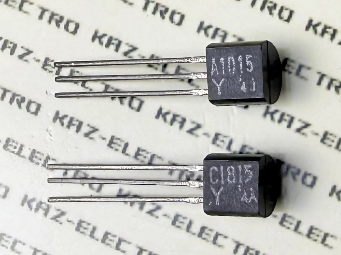
| Toshiba recommended replacement | 2SA1015 (first appeared 1988) ※Some sources list 2SA970 — discrepancy noted |
2SC2240 |
Source: TOSHIBA Semiconductor Databook 1980/1983/1986; Toshiba Semiconductor Databook 1988 Small-Signal Transistors edition;
Transistor Compatibility Reference (『最新トランジスタ互換表』, CQ Publishing, 1980–1988); Transistor Specifications Reference (『最新トランジスタ規格表』, CQ Publishing, 1975–1989)
For a summary of compatible replacements, refer to Chapter 13 “Compatible Device Selection Guide.”
Production Continued Beyond the NRND Designation
Even after the NRND designation in September 1988, production of the 2SA493GTM did not stop immediately. The author has in hand an actual specimen of the 2SA493GTM bearing a lot mark indicating manufacture in January 1991 (Fig. 5-4a, 5-4b).
A word about how it came to be obtained. In 1992, the author — then a student — was eager to get hold of the 2SA493, complementary pair to the 2SC1000. No matter how many electronics shops the author visited, it was nowhere to be found. Heading directly to a Toshiba Service Station at last, what appeared was the 2SA493GTM — the original type had already vanished entirely, and only the GTM type remained available for repair supply.
From this personal experience, combined with the lot mark on the physical device, it appears highly likely that the 2SA493GTM continued to be produced for at least three years after the September 1988 NRND designation. This is one illustration showing that repair supply through Toshiba’s service network was maintained for some time after the official NRND announcement. The same phenomenon has been observed in other GTM variants as well (see Section 10.5.4).
5.5 Discussion
Comparison with the G-Type
This section compares the G-type (TO-98) and GTM-type (TO-92) in terms of maximum ratings, electrical characteristics, and hFE–Ic curves.
| Parameter | 2SA493G/2SC1000G (TO-98: 1977) |
2SA493GTM/2SC1000GTM (TO-92: 1980) |
|---|---|---|
| Vcbo (V) | -50/55 | -50/60 |
| Vceo (V) | -50/50 | -50/50 |
| Ic (A) | -0.05/0.1 | -0.15/0.15 |
| Pc (W) | 0.2/0.2 | 0.4/0.4 |
| hFE | 120-700/200-700 | 120-400/200-700 |
| NF (dB) | Max.2 (120Hz/100Hz) | Max.2 (100Hz) |
| Cob (pF) | 6/6 | 6/6 |
| fT (MHz) | 80/80 | 80/80 |
Source: TOSHIBA Semiconductor Databook 1977/1980
Revised Electrical Specifications
The GTM type inherits the G-type’s core specifications, yet shows significant changes not only in package outline but also in maximum ratings.
While the author refrains from reproducing datebook graphs directly here, the characteristic curves published in the datebook — including the hFE–Ic curve — show considerable differences as well. There are signs of a substantial update involving changes to the die or manufacturing process, suggesting that this was not simply a “change of clothes” but a redefinition that warranted a distinct part number. The details will be examined in Chapter 11.
[Chapter 5 Summary]
The GTM type inherits the G-type lineage while showing changes in package, ratings, and characteristics. Details will be verified in Chapter 11.
→ Next chapter: An examination of the 2SC1000TM — a variant not listed in any official datebook.
6. 2SC1000TM — The Part Without a Datasheet
Chapter contents: A TO-92 variation with no official datasheet or datebook listing. An examination of why it existed, the context surrounding it, and whether a complementary pair “2SA493TM” ever existed.
6.1 A Mysterious Presence
As described in Chapter 5, the G-grade parts of the 2SA493/2SC1000 family were relaunched as “2SA493GTM/2SC1000GTM” for their TO-92 transition, continuing production after 1980. However, a non-G-grade — that is, what appears to be consumer-grade — “2SC1000TM” also exists in the real world. (For a complete list of TM family variants, refer to Section 10.5.2.)
Three peculiarities characterize this device:
- Its specifications were never disclosed — No ratings or characteristics appear in any datebook or catalog.
- And yet it exists — The part number appears only in NRND/DISCON product lists, and the author holds actual specimens.
- Furthermore, production appears to have continued even after the DISCON designation — Physical specimens exist with lot marks dated after the official announcement.
In fact, this is not unique to the 2SC1000TM. Around 1980, as TO-98 devices were being transitioned to TO-92, a number of parts were converted to TO-92 (given the TM suffix) without their datasheets ever being published. The author refers to these as “unlisted-datasheet TM devices.” (A list of such parts follows in Section 6.3.)
The author holds many of these unlisted-datasheet TM devices, including the 2SC1000TM itself, and from the combined observations of all these specimens, estimates that the overall transition unfolded roughly as follows: retirement of TO-98 → bridging by unlisted-datasheet TM parts → full migration to TO-92. This was, in effect, a three-phase handoff.
| Period | TO-92 (New Products) | TO-98 (Legacy Products) | Unlisted-Datasheet TM Products (TO-98→TO-92) * |
|---|---|---|---|
| 1976–1977 | Early stage: new products begin appearing in TO-92 | Peak production: mass production as primary lineup | —— |
| 1978–1979 | Growth stage: production lines gain momentum | Maintained: mass production continues as legacy supply | Introduction: TO-92 conversion underway |
| 1980–1981 | Established: mass production meets TO-98 replacement demand | Wind-down: limited production continues as maintenance supply | Sustained: mass production as replacement supply |
| 1982–1984 | Expansion: active rollout of new discrete products | —— | Wind-down: gradual production cuts as demand eases |
* Unlisted-datasheet TM devices (TO-98→TO-92): devices converted from TO-98 to TO-92 without datasheet publication. Referred to in this text as “unlisted-datasheet TM devices.”
※ The boundaries between phases were not sharply defined; in practice, there was gradual overlap between them. The technical background of the package process transition is discussed in detail in Chapter 10.
The 2SC1000TM fits squarely within this progression. Its first appearance in a Toshiba datebook is in the 1980 edition, in the NRND/DISCON product list. The accompanying notice reads: “As of April 1979 (Showa 54), the following devices have been designated NRND or discontinued. We ask that new designs adopt the recommended replacement devices.” The 2SC1000TM is listed there as the replacement for the 2SC1000 (TO-98). In the 1983 edition’s same list, the 2SC1000TM itself is then treated as a discontinued device.
The author’s observations of the 2SC1000TM specimens on hand are consistent with this account:
- hFE ranks: At minimum, both GR and BL ranks have been confirmed (consistent with the 2SC1000GTM).
- Production period: Units dated to both 1980 and 1982 have been confirmed.
In other words, there is a gap between the official “DISCON” announcement and the actual supply situation on the ground. Today, product lifecycles are managed through clearly defined phases — NRND, EOL, DISCON. At the time, however, the definitions and practical application of “maintenance product” and “discontinued product” appear to have been somewhat loose.
6.2 Why Did It Exist?
What necessitated the “three-phase handoff” described in Section 6.1? The author considers the possible background.
The 1960s–1970s were an era of exponential growth in transistor demand, driven by semiconductor technology advancing at a relentless pace. Toshiba, then at the forefront of resin-encapsulated silicon transistors, was releasing new products one after another. As seen with the 2SC370–374 series — five variants released ranked by hFE alone — fine-grained sales strategies likely contributed to new customer acquisition, though at the cost of an ever-expanding product lineup.
Toshiba wanted to rationalize and slim down this portfolio. But with demand robust and sales strong, production could not simply be halted at the manufacturer’s discretion.
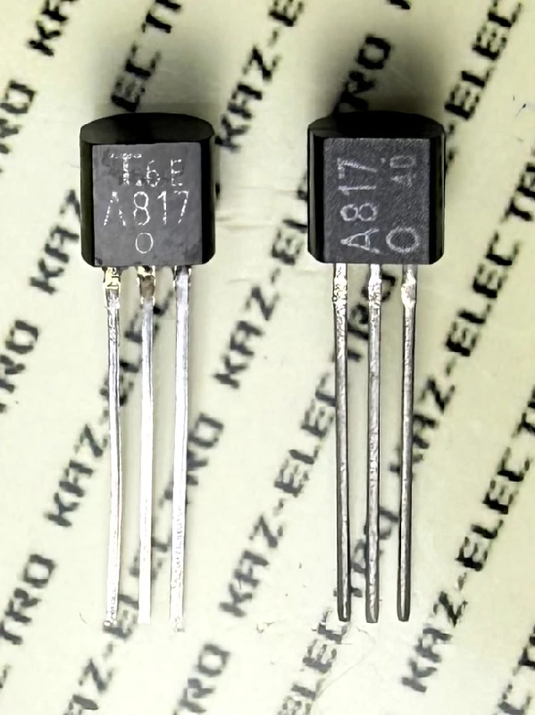
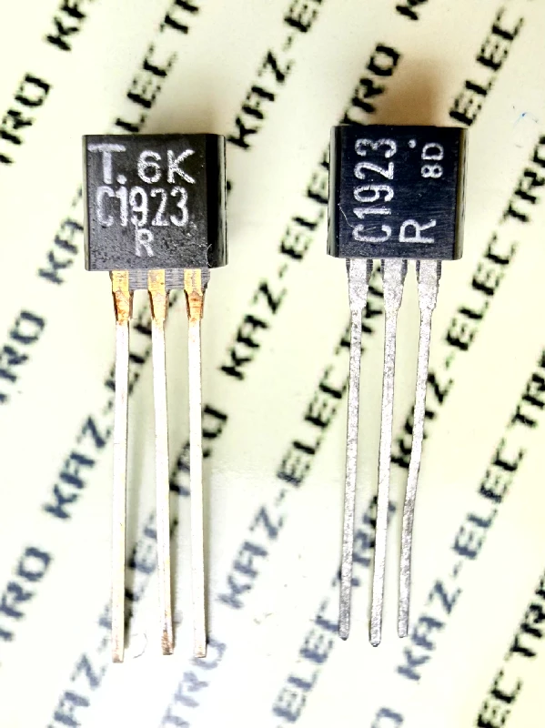
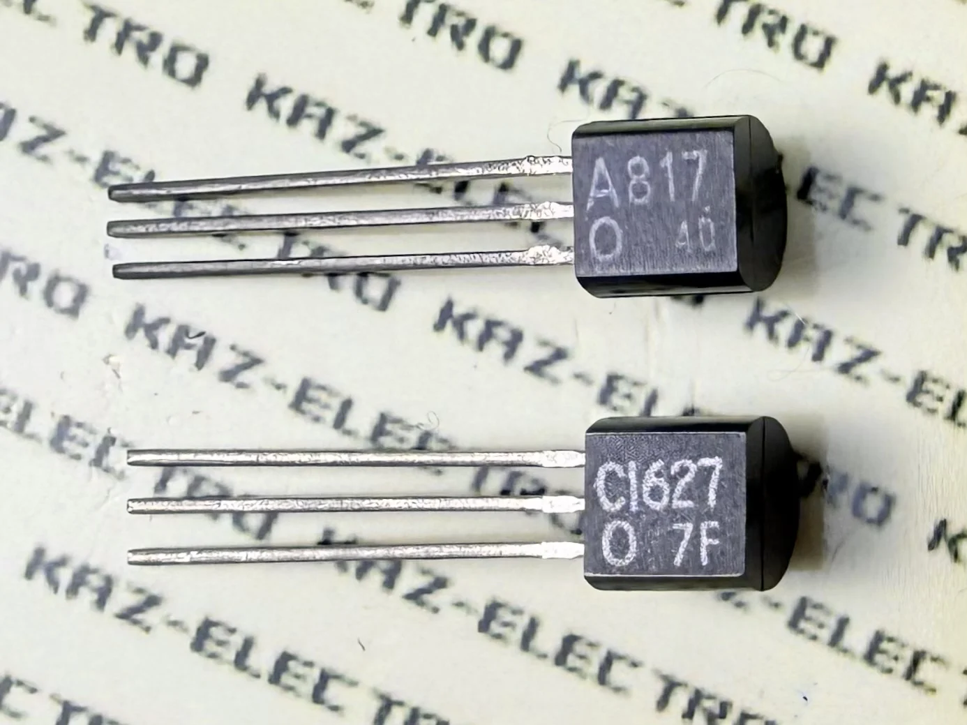
Meanwhile, manufacturing technology was steadily improving. Introduced in the 1977 datebook (published in 1976): the 2SA817/2SC1627, the 2SC1815 (with 2SA1015 first appearing in the 1980 datebook), the 2SC1923, and the 2SC1959 — all new-generation devices that debuted from the outset in TO-92. The 2SA493/2SC1000 family was still in its TO-98 era. The photographs show early lot specimens from 1976; physical survivors from this period are extremely rare.
All of these went on to survive until Toshiba’s major discrete device consolidation in 2012 — and it is telling that their initial 1976 appearance carried the same printing style as TO-98 parts.
With its transfer molding production lines now expanded, Toshiba channeled strong customer demand toward these new products while continuing to supply the legacy TO-98 parts — now repackaged in TO-92 with the TM suffix — to meet existing users’ needs. The unlisted-datasheet TM devices were, the author believes, born as a stopgap to facilitate this transition smoothly.
6.3 List of Unlisted-Datasheet TM Devices
As noted in Section 6.1, the 2SC1000TM is not an isolated exception. The following is a list of unlisted-datasheet TM devices confirmed from the NRND/DISCON product lists in Toshiba databooks.
| PNP | NPN |
|---|---|
| 2SA495TM | 2SC372TM |
| 2SA509TM | 2SC509TM |
| 2SA561TM | 2SC734TM |
| 2SA661TM | 2SC1161TM |
| 2SA841TM | 2SC1681TM |
| 2SA842TM | 2SC1682TM |
| — | 2SC373TM |
| — | 2SC380ATM |
| — | 2SC381TM |
| — | 2SC385ATM |
| — | 2SC387ATM |
| — | 2SC394TM |
| — | 2SC733TM |
| — | 2SC735TM |
| — | 2SC784TM |
| — | 2SC785TM |
| — | 2SC983TM |
| — | 2SC1000TM |
These devices, like the 2SC1000TM, are confirmed as part number entries in NRND/DISCON lists only; no datasheet was provided for any of them. Detailed specifications are unknown, but they are presumed to carry ratings and electrical characteristics at least equivalent to the original type number they replaced.
As a brief aside, let the author touch on a few companions of the 2SA493/2SC1000 — devices born for audio use.
2SA561TM / 2SC734TM
First, the TM-converted versions of the 50V-class driver amplifier pair 2SA561/2SC734 (50V / 0.15A / 0.3W / fT 70–150MHz) — ancestors, in a sense, of the later 2SA1015/2SC1815. They also appear in Section 7.1.2.
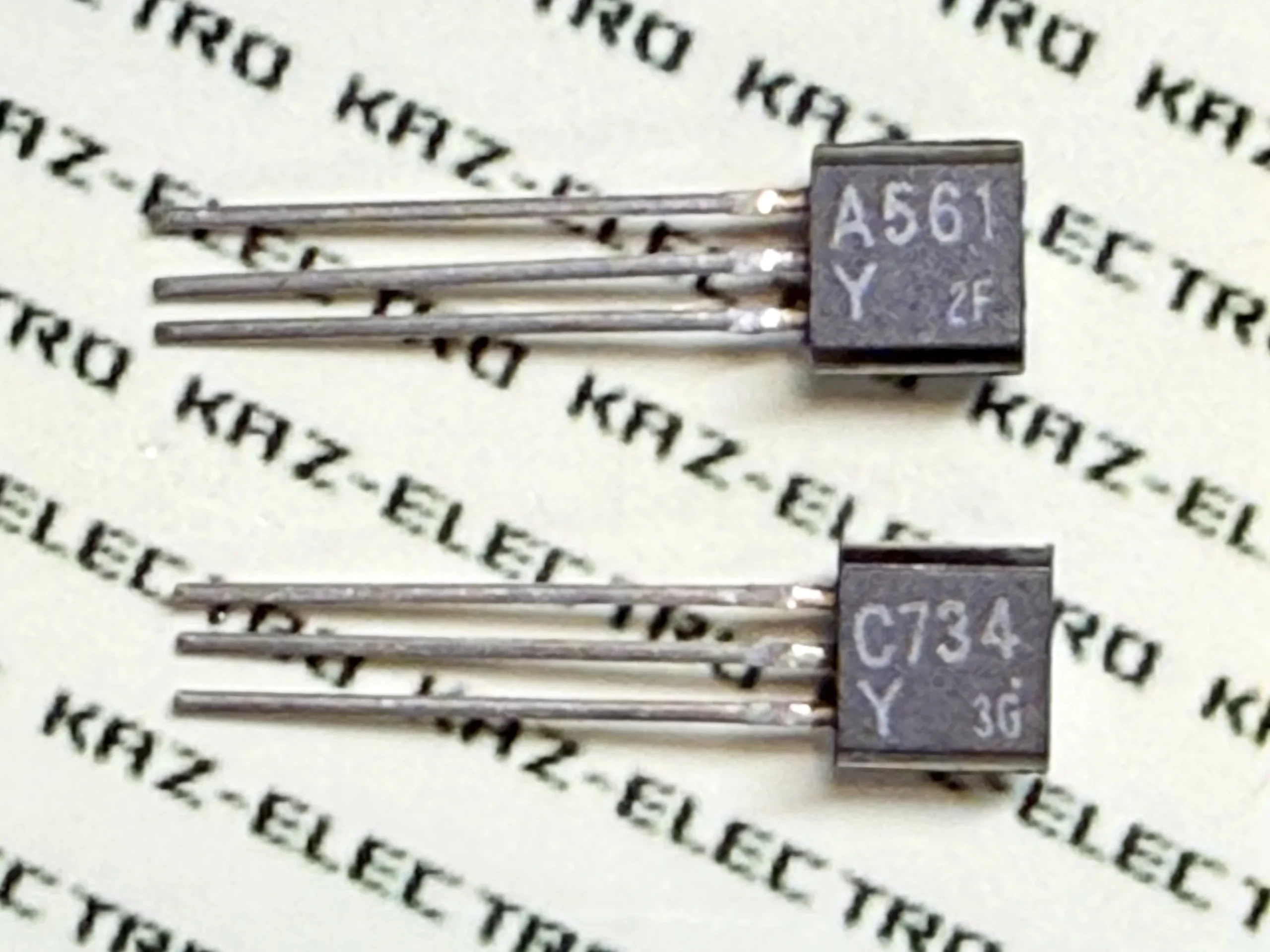
2SA661TM / 2SC1166TM
Likewise, the TM-converted versions of the 50V-class 2SA661/2SC1166 (50V / 0.2A / 0.6W / fT 100–120MHz) — predecessors of the 2SA817/2SC1627, a complementary pair that would go on to last roughly 35 years. Housed in Toshiba’s proprietary rectangular package “TOSHIBA 2-5S” with a notably thick collector lead, these were designed to handle higher drive currents than the 2SA561/2SC734. This distinctive rectangular package was also transitioned to TM during the same period.
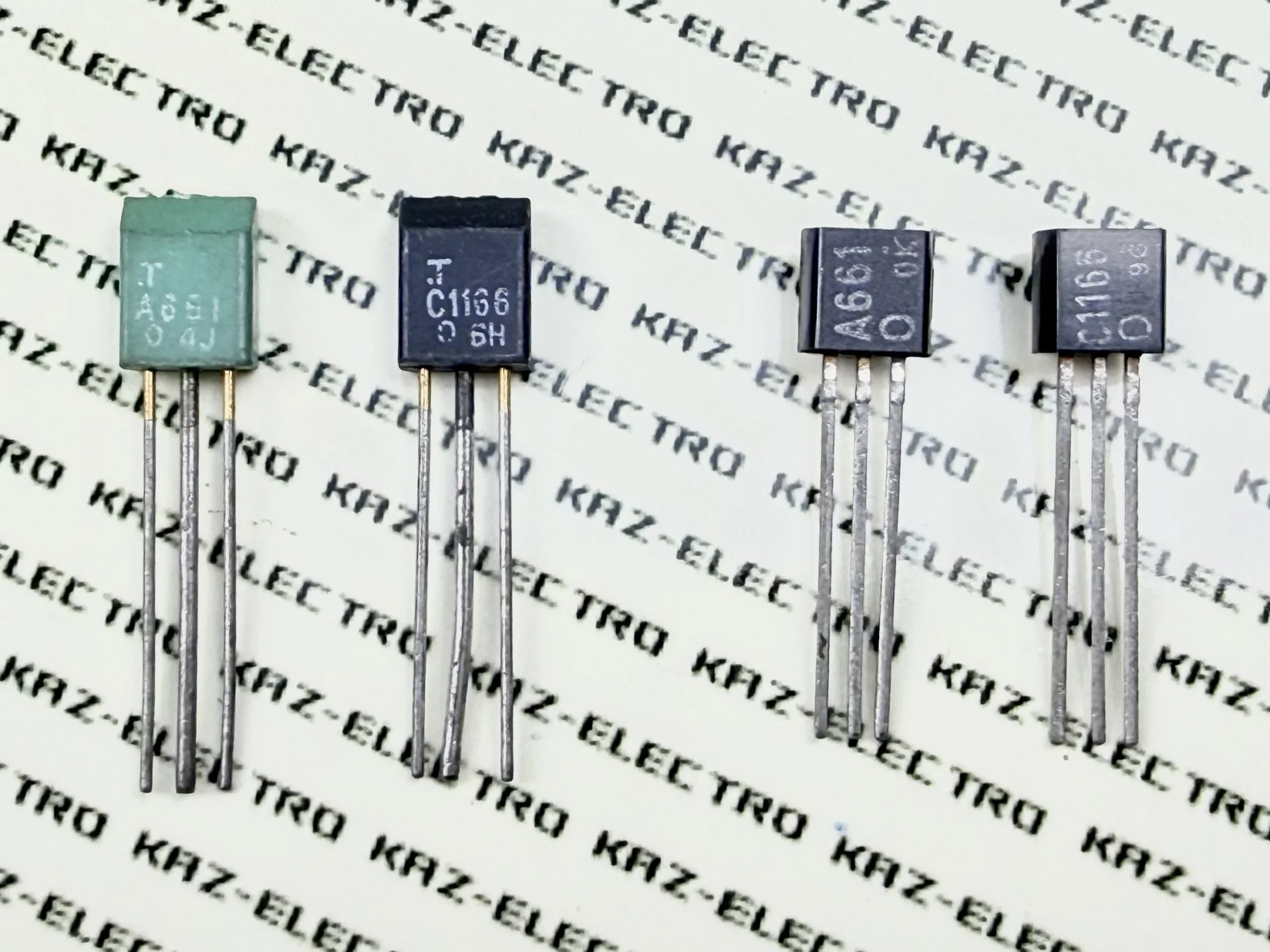
All of these occupy the same position as the 2SC1000TM examined in this chapter. Amidst the sweeping wave of TO-98 discontinuation, they were quietly converted to TM — without datasheets — and lived on for a while. Most appear to have had only a brief production run of roughly 1980–1983, consistent with both the author’s observations of physical specimens and the records in Toshiba databooks. A few exceptions proved more resilient; these will be revisited in Section 10.5.4.
6.4 Does the 2SA493TM Exist?
The Toshiba datebook NRND/DISCON lists contain no entry for “2SA493TM.” As far as the records show, it does not exist. But why?
6.4.1 A Difference in Market Segments
From their debut, the 2SA493/2SC1000 were sold in parallel as the industrial grade (G-series) and the consumer grade (plain type). The two followed different fates.
6.4.2 Fierce Competition in the Consumer (Audio) Market
The late 1970s were the height of the audio boom. Manufacturers were releasing new high-performance low-noise transistors in rapid succession, driving an intense development race.
In this environment, the plain 2SA493 became visibly obsolete in performance terms and disappeared from the market early. Audio equipment manufacturers shifted their designs one after another to newer, higher-performance parts. With nowhere left to go, the 2SA493 quietly faded away.
The complementary pair 2SC1000 (plain type) also received an NRND designation in 1980 — but, perhaps because demand for it as a general-purpose high-hFE NPN transistor extended beyond audio applications, it was briefly TM-converted and production continued for a short time.
The 2SA493, by contrast, existed primarily as a low-noise transistor for audio use, and its reason for being diminished in the face of newer products. The author believes there was simply no need to TM-convert it.
6.4.3 The Conservative Nature of the Industrial (Telecom/Industrial) Equipment Market
Industrial applications were a different story entirely. Broadcast, communications, and measurement equipment does not undergo model changes as frequently as consumer products, and these devices are used over long periods with maintenance and servicing. This means that stable long-term supply of components is strongly required.
The 2SA493G was widely adopted in industrial applications, and maintenance demand continued over the long term. The author therefore infers that it was TM-converted and continued to be manufactured until around 1991, even after TO-98 production ended.
In industrial applications, there was no need for a “latest model” like the 2SA970. The proven 2SA493G was sufficient.
6.4.4 Conclusion
From these circumstantial indicators, the author believes the 2SA493TM most likely does not exist:
- Consumer equipment demand had already disappeared early on
- Industrial equipment demand was handled by the G-series (GTM)
- → There was no need for a TM conversion
That said, some devices not listed in datebook NRND/DISCON tables do physically exist — and the author holds specimens:
- 2SA429TM / 2SC780ATM
- 2SA562TM-GR / 2SC1959-GR
- 2SC732TM-V
2SA562TM / 2SC1959
Of these, the 2SA562TM / 2SC1959 have officially listed hFE ranks of only O (70–140) and Y (120–240) in the datebook. Based on Toshiba’s rank assignment conventions, the GR rank is estimated to be 200–400.
2SC732TM
For the 2SC732TM as well, the datebook lists only GR (200–400) and BL (350–700) officially. Following Toshiba’s conventions, V is estimated at 600–1200.
These undocumented hFE rank variants are a phenomenon seen even in the TO-98 era of the 1960s–70s, and appear sporadically in TO-92 devices from the early 1980s as well. This is perhaps a peculiarity of the era when discrete devices were indispensable.
Most of these circulated only through junk component shops, and the author believes they were custom-order parts for large-volume buyers that found their way onto the surplus market. Given that such examples exist even among TO-92 parts, the possibility that a 2SA493TM exists cannot be entirely ruled out.
If you happen to have a physical specimen of the 2SA493TM, the author would very much like to hear from you.
The 2SC1000TM is a mysterious device — no datasheet was ever published. Yet its part number is confirmed in Toshiba datebook NRND/DISCON lists, and it did circulate in the general market, albeit briefly. Based on observations of physical specimens, production is estimated to have taken place roughly between 1978 and 1984.
The background lies in the shutdown of TO-98 production lines around 1980. The 2SC1000TM appears to have emerged in response to persistent market demand for a substitute for the 2SC1000, serving as a bridge to facilitate the transition to the next generation.
The complementary pair 2SA493, meanwhile, lost its presence amid the fierce development race in the consumer audio market and most likely disappeared without ever being TM-converted.
The 2SA493TM — in all probability, it does not exist. Yet devices not listed in databooks do occasionally surface from junk shops. The author remains open to any information.
→ Next chapter: PCT technology and an investigation into the development history.
7. Before the Low-Noise Complementary Pair Arrived — An Early Registration Number, a Late Debut
The EIAJ registration numbers for the 2SA493/2SC1000 are low. And yet volume production did not begin until 1971 — late by the standards of contemporary devices. Behind this pattern of an early registration number but a late debut lay not only the fundamental requirement of low noise but the need to simultaneously satisfy the following technical conditions:
- The hFE barrier inherent to silicon PNP — Silicon PNP is harder to manufacture with high hFE compared to NPN, with lower yields. Securing the “high gain” that is a prerequisite for low-noise devices was itself difficult.
- The tension between high breakdown voltage and low noise — Pushing the breakdown voltage to the 50V class increases collector cutoff current (ICBO) and surface leakage current, both of which become noise sources. At the time, this effect applies equally to NPN and PNP as a fundamental semiconductor phenomenon. However, due to structural disadvantages inherent to PNP devices — such as lower hole mobility — the design margin for simultaneously achieving high breakdown voltage and low noise was narrower, making the challenge more acute for PNP in practice.
- The tension between resin encapsulation and low noise — Resin, being less hermetic than metal, allows moisture ingress that increases surface leakage current. It is an unfavorable package for low-noise chips that are sensitive to moisture and contaminants.
- The barrier to forming a complementary pair — The PNP described in constraints 1–3, with all its limitations, had to be manufactured to match characteristics with the NPN.
Any one of these hurdles, in isolation, might have been solvable. The four together raised the difficulty to a different order. This article refers to them as “The Four Technical Hurdles.” This chapter examines these hurdles through evidence drawn from the broader landscape of Toshiba silicon PNP devices, the development activities of competing manufacturers, and analysis of registration numbers.
7.1 Analysis of the Release Delay
7.1.1 When Did the 2SA493/2SC1000 First Appear?
The first appearance of the 2SA493/2SC1000 in official records is the 1973 Toshiba Semiconductor Handbook (東芝半導体ハンドブック), published in November 1972. The preceding 1971 edition (published 1970) does not list them. If this 1973 edition listing is taken as the “official debut,” then a considerable amount of time had passed since the registration of the part numbers.
What is EIAJ?
EIAJ (Electronic Industries Association of Japan) was Japan’s electronics industry association, responsible for semiconductor part-number registration (2SA, 2SC, etc.) in Japan. Manufacturers applied to EIAJ at the product planning stage to reserve their numbers. In 2000, EIAJ was merged into JEITA (Japan Electronics and Information Technology Industries Association).
The actual market introduction, however, was somewhat earlier. This site estimates that full-scale volume production began in 1971.
Two pieces of evidence support this. First, the Toshiba Vacuum Tube, Semiconductor, and Integrated Circuit Handbook (東芝 真空管・半導体・集積回路ハンドブック), published in 1971, carries the listing. Second, the first appearance in Transistor Compatibility Reference (『最新トランジスタ互換表』, CQ Publishing) also dates to 1971.
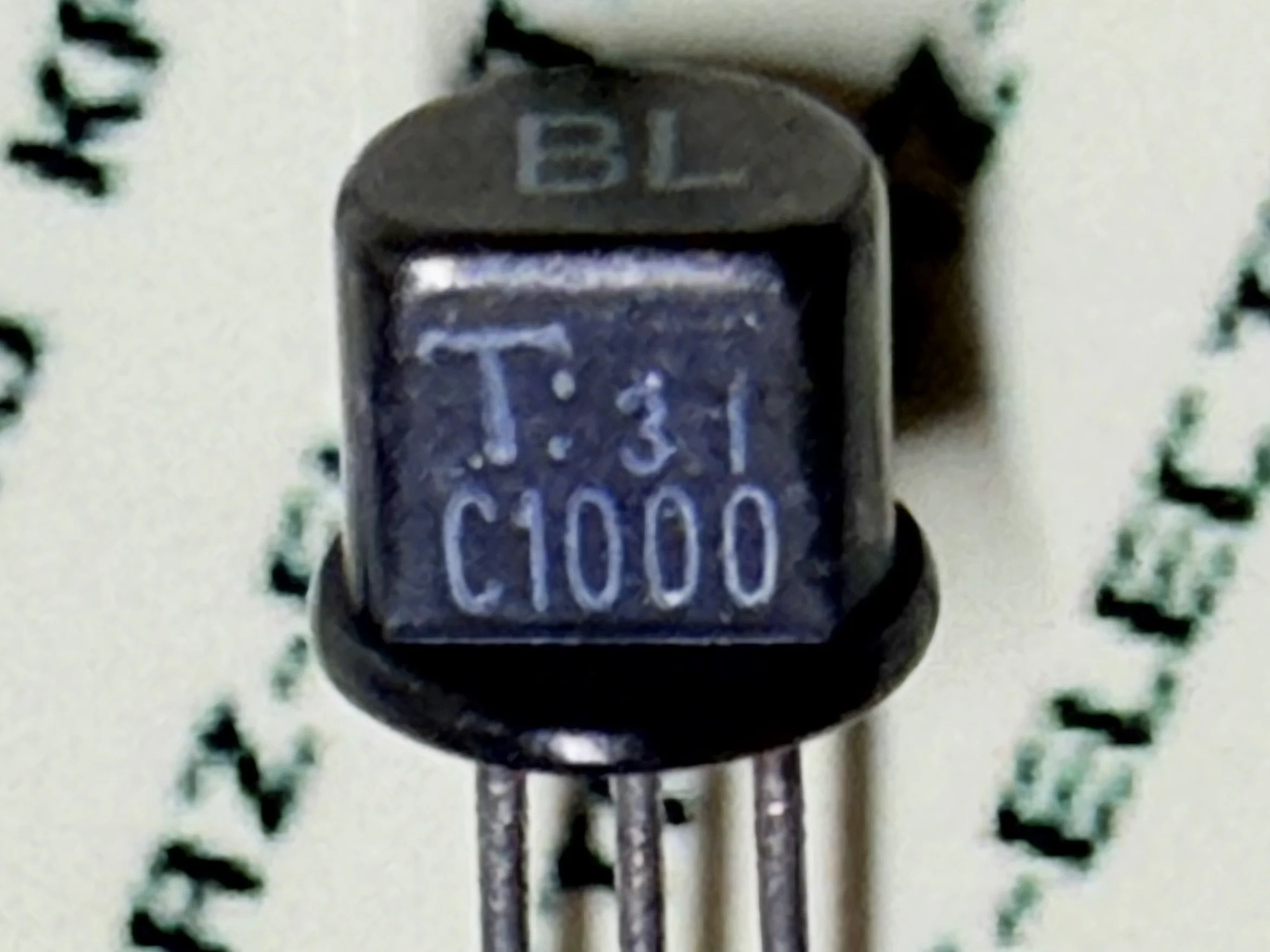
Furthermore, back-calculating EIAJ registration year from the part number raises the possibility that physical specimens manufactured between 1966 and 1970 exist. In fact, this site holds multiple specimens bearing katakana lot markings.
The 2SC1000 shown above carries the lot mark “エ” and is estimated to have been manufactured in December 1969 — the oldest specimen this site holds.
Toshiba used lowercase Roman letters, hiragana, and katakana as lot markings from the 1960s through June 1973. This is estimated from observations of several thousand Toshiba TO-98 physical specimens held by this site. Research into Toshiba’s lot marking conventions is ongoing; findings will be reported separately when complete.
During the 1960s, mass production processes had not yet stabilized, and it is conceivable that supply was limited to a small number of users in small quantities — though this too remains the site’s inference.
Bringing these threads together, three possibilities emerge for the start of mass production of the 2SA493/2SC1000 (i.e., the date of its appearance in the general market):
- 1972: First listed in the 1973 Toshiba Semiconductor Handbook (published November 1972)
- 1971: Included in the Toshiba handbook published that year and in Transistor Compatibility Reference (『最新トランジスタ互換表』, CQ Publishing)
- Before 1969: The oldest lot mark held by this site dates to December 1969 (estimated)
Accounting for objectivity, option 2 — assuming volume production began around 1971 — appears most defensible.
7.1.2 Why Is This Considered Late?
Assuming volume production began in 1971, was that actually late? The answer, plainly, is yes. Comparing against Toshiba’s own development timeline makes the delay concrete.
Silicon transistors are easier to manufacture as NPN than as PNP. Looking first at the NPN side: Toshiba’s first silicon low-noise NPN, the 2SC369 (30V), had already been in volume production since 1965. The 2SC1000 appeared a full six years later.
The part numbering itself reveals an anomaly. Toshiba had already released the 2SC1001 through 2SC1004 — the numbers immediately following 2SC1000 — as early as 1970. The 2SC1001–1003 are silicon NPN medium-power transistors in TO-39 packages: fT of 350–700MHz, IC = 0.5–2A, VCBO = 36–40V, PC = 5–20W — high-frequency power amplifiers. The specification of 1.5W output in the UHF 470MHz band represents a development challenge incomparably greater than the low-frequency small-signal 2SC1000. Their part numbers are just one step above 2SC1000, yet full volume production began nearly a year earlier.
The 2SC1004 is a silicon NPN power transistor in TO-3, rated VCBO = 1100V, IC = 0.5A, PC = 50W — an ultra-high-voltage device for CRT television sets. All of the 2SC1001–1004 carry state-of-the-art specifications for their era and represent greater development difficulty than the 2SC1000. Yet all entered volume production before it.
This was the delay even for NPN, which is easier to manufacture. On the PNP side the pattern is even more pronounced. Toshiba’s first silicon complementary pair, the 2SA500/2SC400 (TO-18, 20V), appeared in 1965. By registration number, the 2SA493 precedes the 2SA500 (493 < 500) — yet volume production began six years later.
The following table organizes Toshiba’s complementary pair development chronology.
| Type | Year | Significance |
|---|---|---|
| 2SA493/2SC1000 | 1971 | Japan’s first 50V low-noise complementary pair |
| 2SA494G/2SC369G | 1970/1966 | Japan’s first low-noise complementary pair |
| 2SA500/2SC400 | 1965 | Japan’s first silicon complementary pair |
| 2SA561/2SC734 | 1968 | Japan’s first 50V complementary pair |
This timeline shows that the 2SA493/2SC1000 is a product simultaneously satisfying three requirements — “50V,” “low noise,” and “complementary” — and that even counting from the devices that had achieved each requirement individually, it took three to six years. This suggests that multiple technical hurdles stood between the design goals and volume production of a transistor meeting all three criteria at once.
7.1.3 The Full Picture of Toshiba Silicon PNP
The previous section established, from Toshiba’s complementary pair timeline, that the 2SA493/2SC1000 debuted late. But why? To find clues, this section surveys all Toshiba silicon PNP devices in the 2SA400-series chronologically.
The era of the 2SA 400-series was a time when germanium transistors still dominated. Silicon transistors were just beginning to appear sporadically, in a dawn period — and by EIAJ registration number, the 2SA493 became Japan’s first “silicon PNP low-noise transistor.” It was a product Toshiba had held in reserve until the moment was right.
The 2SA493 was only the third silicon PNP in TO-98. So why, as the “third,” was volume production as late as 1971? The table below shows the full picture of Toshiba silicon PNP releases at the time.
| No. | PNP Type | NPN Type | VCEO | Package | Year | Notes |
|---|---|---|---|---|---|---|
| 1 | 2SA429G | 2SC780AG | 150V | TO-98 | 1968 | High voltage |
| 2 | 2SA467G | 2SC366G | 30V | TO-98 | 1968 | |
| 3 | 2SA493 | 2SC1000 | 50V | TO-98 | 1971 | Article subject — 50V low-noise |
| 4 | 2SA494 | 2SC369 | 30/18V | TO-98 | 1970 / 1965 | Sister device, low-noise 30V |
| 5–6 | (abbreviated: 2SA495, 2SA499 — see full timeline below) | |||||
| 7 | 2SA500 | 2SC400 | 20V | TO-18 | 1965 | Toshiba’s first silicon complementary pair |
From this summary table, the anomalous delay of the 2SA493 becomes concrete. Among TO-98 small-signal transistors, the 2SA493 is only the third device — yet the 2SA429G (first) and 2SA467G (second), registered later than the 2SA493 by number, entered volume production earlier. This is the archetypal instance of the “earlier registration, later debut” pattern described in Section 7.1.2.
This divergence between registration order and production order is not limited to the 2SA493. Toshiba registered a concentration of silicon PNP devices in the 2SA400-series, but many of them required considerable time to reach volume production. The full table below shows the complete picture.
| No. | Type | VCEO | Package | Year | ’65 | ’66 | ’67 | ’68 | ’69 | ’70 | ’71 | ’72 | ’73 | ’74 | ’75 | ’76 | ’77 | ’78 | ’79 |
|---|---|---|---|---|---|---|---|---|---|---|---|---|---|---|---|---|---|---|---|
| 1 | 2SA429G | 150 | TO-98 | 1968 | ■ | ■ | ■ | ■ | ■ | ■ | ■ | ■ | ■ | ■ | ■ | ■ | |||
| 2SC780AG | 150 | 1972 | ■ | ■ | ■ | ■ | ■ | ■ | ■ | ■ | |||||||||
| 2 | 2SA467G | 30 | TO-98 | 1968 | ■ | ■ | ■ | ■ | ■ | ■ | ■ | ■ | ■ | ■ | ■ | ■ | |||
| 2SC366G | 40 | 1965 | ■ | ■ | ■ | ■ | ■ | ■ | ■ | ■ | ■ | ■ | ■ | ■ | ■ | ■ | ■ | ||
| 2SC367G | 20 | 1965 | ■ | ■ | ■ | ■ | ■ | ■ | ■ | ■ | ■ | ■ | ■ | ■ | ■ | ■ | ■ | ||
| 3 | 2SA473 | 30 | TO-220 | 1972 | ■ | ■ | ■ | ■ | ■ | ■ | ■ | ■ | |||||||
| 2SC1173 | 1972 | ■ | ■ | ■ | ■ | ■ | ■ | ■ | ■ | ||||||||||
| — | 2SA481 | — | number only | — | |||||||||||||||
| 4 | 2SA482 | — | TO-39 | — | |||||||||||||||
| 5 | 2SA483 | 150 | TO-66 | 1972 | ■ | ■ | ■ | ■ | ■ | ■ | ■ | ■ | ■ | ■ | |||||
| 2SC783 | 200 | 1968 | ■ | ■ | ■ | ■ | ■ | ■ | ■ | ■ | ■ | ■ | ■ | ■ | |||||
| 6 | 2SA484 | 110 | TO-39 | 1968 | ■ | ■ | ■ | ■ | ■ | ■ | ■ | ■ | ■ | ■ | ■ | ■ | |||
| 2SC484 | 110 | 1968 | ■ | ■ | ■ | ■ | ■ | ■ | ■ | ■ | ■ | ■ | ■ | ■ | |||||
| 7 | 2SA485 | 80 | TO-39 | 1968 | ■ | ■ | ■ | ■ | ■ | ■ | ■ | ■ | ■ | ■ | ■ | ■ | |||
| 2SC485 | 80 | 1968 | ■ | ■ | ■ | ■ | ■ | ■ | ■ | ■ | ■ | ■ | ■ | ■ | |||||
| 8 | 2SA486 | 50 | TO-39 | 1968 | ■ | ■ | ■ | ■ | ■ | ■ | ■ | ■ | |||||||
| 2SC486 | 50 | 1968 | ■ | ■ | ■ | ■ | ■ | ■ | ■ | ■ | |||||||||
| — | 2SA487 | — | number only | — | |||||||||||||||
| — | 2SA488 | — | number only | — | |||||||||||||||
| 11 | 2SA489 | 60 | TO-220 | 1972 | ■ | ■ | ■ | ■ | ■ | ■ | ■ | ■ | |||||||
| 2SC789 | 60 | 1972 | ■ | ■ | ■ | ■ | ■ | ■ | ■ | ■ | |||||||||
| 12 | 2SA490 | 40 | TO-220 | 1972 | ■ | ■ | ■ | ■ | ■ | ■ | ■ | ■ | |||||||
| 2SC790 | 40 | 1972 | ■ | ■ | ■ | ■ | ■ | ■ | ■ | ■ | |||||||||
| 13 | 2SA493 | 50 | TO-98 | 1971 | ■ | ■ | ■ | ■ | ■ | ■ | ■ | ■ | ■ | ||||||
| 2SC1000 | 50 | 1971 | ■ | ■ | ■ | ■ | ■ | ■ | ■ | ■ | ■ | ||||||||
| 2SA493G | 50 | TO-98 | 1972 | ■ | ■ | ■ | ■ | ■ | ■ | ■ | ■ | ||||||||
| 2SC1000G | 50 | 1972 | ■ | ■ | ■ | ■ | ■ | ■ | ■ | ■ | |||||||||
| 14 | 2SA494﹡ | 30 | TO-98 | 1970 | ■ | ■ | ■ | ■ | |||||||||||
| 2SC369﹡ | 18 | 1965 | ■ | ■ | ■ | ■ | ■ | ■ | ■ | ||||||||||
| 2SA494G | 30 | TO-98 | 1970 | ■ | ■ | ||||||||||||||
| 2SC369G | 18 | 1965 | ■ | ■ | ■ | ■ | ■ | ■ | ■ | ■ | ■ | ||||||||
| 15 | 2SA495 | 30 | TO-98 | 1968 | ■ | ■ | ■ | ■ | ■ | ■ | ■ | ■ | ■ | ■ | ■ | ■ | |||
| 2SC372 | 30 | 1965 | ■ | ■ | ■ | ■ | ■ | ■ | ■ | ■ | ■ | ■ | ■ | ■ | ■ | ■ | ■ | ||
| 16 | 2SA496 | 30 | TO-126 | 1968 | ■ | ■ | ■ | ■ | ■ | ■ | ■ | ■ | ■ | ■ | ■ | ■ | |||
| 2SC496 | 30 | 1968 | ■ | ■ | ■ | ■ | ■ | ■ | ■ | ■ | ■ | ■ | ■ | ■ | |||||
| 17 | 2SA497 | 80 | TO-39 | 1968 | ■ | ■ | ■ | ■ | ■ | ■ | ■ | ■ | ■ | ■ | ■ | ■ | |||
| 2SC497 | 80 | 1968 | ■ | ■ | ■ | ■ | ■ | ■ | ■ | ■ | ■ | ■ | ■ | ■ | |||||
| 18 | 2SA498 | 80 | TO-39 | 1968 | ■ | ■ | ■ | ■ | ■ | ■ | ■ | ■ | ■ | ■ | ■ | ■ | |||
| 2SC498 | 80 | 1968 | ■ | ■ | ■ | ■ | ■ | ■ | ■ | ■ | ■ | ■ | ■ | ■ | |||||
| 19 | 2SA499 | 40 | TO-18 | 1965 | ■ | ■ | ■ | ■ | ■ | ■ | ■ | ■ | ■ | ■ | ■ | ■ | ■ | ■ | ■ |
| 2SC979 | 50 | 1968 | ■ | ■ | ■ | ■ | ■ | ■ | ■ | ■ | ■ | ■ | ■ | ■ | |||||
| 20 | 2SA500 | 20 | TO-18 | 1965 | ■ | ■ | ■ | ■ | ■ | ■ | ■ | ■ | ■ | ■ | ■ | ■ | ■ | ■ | ■ |
| 2SC400 | 20 | 1965 | ■ | ■ | ■ | ■ | ■ | ■ | ■ | ■ | ■ | ■ | ■ | ■ | ■ | ■ | ■ |
Note: ■ = in production (including NRND period). “—” = registered number only, no confirmed product. ﹡ = pair not explicitly designated as complementary in datebook. Nos. 9–10 are missing from the sequence.
▼ Show full timeline (20 types)
What the Full Table Reveals
1. Toshiba’s overwhelming early investment
Among silicon PNP complementary pairs registered between 2SA429 and 2SA513, there are no fewer than 29 pairs — and all are Toshiba products. Toshiba developed a broad lineup from small-signal to medium power ahead of any competitor in a single burst. This early investment became the source of competitive advantage in the market years later.
2. Metal-can packages first, resin packages delayed
Complementary pairs in metal-can packages (TO-18, TO-39) were released relatively early. Resin-based packages (TO-98, TO-126, TO-220), by contrast, are uniformly delayed in their release timing.
3. Delays even among voltage-variant siblings
Even among voltage-variant siblings of the same device family, the higher-voltage type tends to appear later. This pattern is not limited to PNP. The diagram below compares by application category.
2SC400 (20V, 1965)
No delay
2SC979 (50V, 1968)
NPN: 3-year delay
NPN: 3-year delay
2SC369G (30V, 1965)
PNP: 5-year delay
NPN: 6-year delay
2SC1000 (50V, 1971)
No delay
※ Years shown are estimates based on Toshiba datebook editions.
The diagram shows that rising manufacturing difficulty with higher breakdown voltages caused delays regardless of polarity. Moving from general-purpose industrial devices to low-noise devices, the delays widen further — and the 6-year lag of the 2SC1000 (the article’s main subject) stands out starkly.
4. Strategic part number reservation
In this era, the 2SA series (predominantly germanium) and the 2SC series (predominantly silicon) were at rough numerical equilibrium in their registration numbers. Germanium was easier to manufacture as PNP; silicon was easier as NPN. And at the time, silicon transistors were still in their growth phase, with PNP registrations lagging NPN. Toshiba appears to have taken advantage of this situation, deliberately reserving part numbers to align complementary pairs. The perfect number-matching in 2SA497/2SC497, 2SA503/2SC503, 2SA509/2SC509, 2SA510/2SC510, and the memorable 2SA500/2SC400, all suggest intentional simultaneous reservation.
When silicon ultimately became the mainstream, the easier-to-manufacture NPN expanded overwhelmingly in variety, with the 2SA series eventually reaching the 2200-series and 2SC reaching the 6000-series. This “miracle” of matching complementary numbers was a phenomenon unique to this era. Toshiba’s rush to secure registrations — even at the cost of production readiness — may itself have been one factor widening the gap between registration order and production order.
7.1.4 How Other Manufacturers Followed
So far this chapter has traced developments within Toshiba. Broadening the view, the author now examines the pace at which contemporaries were introducing complementary pairs.
Surveying the appearance of products from other manufacturers equivalent to the 2SA493/2SC1000 — that is, 50V low-noise complementary pairs in resin packages — NPN devices concentrate in the 1300-series (1972), PNP in the 700-series (1973). Toshiba’s registration number advantage (2SA493/2SC1000) is striking.
| Type | Maker | Year | Significance |
|---|---|---|---|
| 2SA672/2SC1345﹡ | Hitachi | 1972/1972 | Hitachi’s first 50V low-noise PNP/NPN |
| 2SA705/2SC632A | Sony | 1973/1972 | Sony’s first 50V low-noise complementary pair |
| 2SA722/2SC1328 | Matsushita | 1973/1972 | Matsushita’s first 55V low-noise complementary pair |
| 2SA726/2SC1313﹡ | Mitsubishi | 1973/1972 | Mitsubishi’s first low-noise PNP/NPN |
| 2SA750/2SC1400 | NEC | 1973/1974 | NEC’s first 50V low-noise complementary pair |
| 2SA929/2SC1570 | Sanyo | 1978 | Sanyo’s first 50V low-noise complementary pair |
﹡ Not explicitly designated as complementary by the manufacturer, but ratings and characteristics are similar.
At Sony, Matsushita, and Mitsubishi as well, the same tendency is confirmed: PNP appeared later than NPN, just as with Toshiba. This suggests that the technical difficulties in developing 50V-class low-noise complementary pairs were shared across the industry, not unique to Toshiba.
Going further back to the very dawn of silicon complementary pairs, Toshiba’s lead becomes even clearer. As the full table in Section 7.1.3 shows, Toshiba registered 29 silicon complementary pairs with EIAJ between 2SA429 and 2SA513. The early activities of other manufacturers are shown below.
| Maker | PNP Type | NPN Type | Package | Notes |
|---|---|---|---|---|
| Toshiba/Fujitsu | 2SA522N | 2SC595N | TO-39 | Shared by multiple makers ※ |
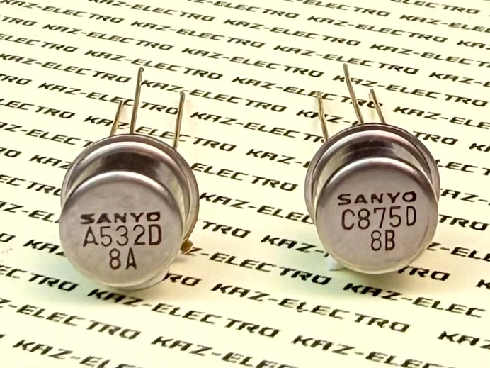
| Sanyo | 2SA532 | 2SC875 | TO-39 | |
| Hitachi | 2SA537 | 2SC708 | TO-39 | |
| NEC | 2SA539 | 2SC815 | TO-92 | Resin package |
| NEC | 2SA544 | 2SC32 | TO-39 | |
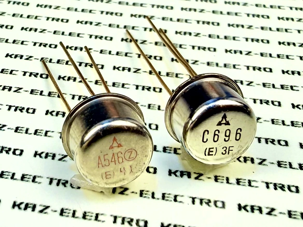
| Matsushita | 2SA546 | 2SC696 | TO-39 | |
| Matsushita | 2SA550 | 2SC538 | TO-18 | Small-signal |
Notably, most of the early complementary pairs from other manufacturers came as single one-off releases of TO-39 medium-power devices. No other manufacturer came close to Toshiba’s breadth — a comprehensive lineup from small-signal to medium power rolled out in one sweep — making Toshiba’s industry leadership in this era unmistakable.
[Column] The “Shared Listing” Phenomenon in EIAJ Numbers
The 2SA522N/2SC595N were manufactured by both Toshiba and Fujitsu. Under EIAJ rules, registered part numbers were shared industry property, and other manufacturers were permitted to produce under the same type number. In practice, however, such “shared listings” occurred in only a handful of devices in this era. The 2SC594, for example, was shared by five manufacturers — Fujitsu, Oki, NEC, Mitsubishi, and Toshiba — but this was an exceptionally rare case.
7.1.5 Technical Causes of the Release Delay
Combining the full table in Section 7.1.3 with the competitor data in Section 7.1.4, the contours of the factors behind the 2SA493/2SC1000 release delay begin to emerge.
Products in metal-can packages (TO-18, TO-39) reached volume production relatively early. The greater the overlap of resin package transition, higher voltage, PNP polarity, and low-noise performance requirements, the more volume production was delayed. Of “The Four Technical Hurdles” discussed in Section 8.2, the combination of “PNP polarity” and “resin package” was most likely the greatest obstacle. Even PNP transistors that could reach volume production in metal-can packages relatively early became dramatically more difficult once resin encapsulation entered the picture. The “anomalously late debut” of the 2SA493/2SC1000 speaks plainly to this technical difficulty.
Source: Toshiba Semiconductor Databook, various years; Transistor Compatibility Reference (『最新トランジスタ互換表』, CQ Publishing), various years
Despite its low EIAJ registration number, full-scale volume production of the 2SA493/2SC1000 is estimated to have begun in 1971. Behind this “anomalously late debut” lay The Four Technical Hurdles: the hFE barrier inherent to PNP, the tension between high breakdown voltage and low noise, the tension between resin encapsulation and low noise, and the barrier to forming a complementary pair. Of these, the combination of “PNP polarity” and “resin package” was the greatest obstacle. The PCT technology that formed the manufacturing foundation for this achievement is discussed in detail in Section 9.2.
→ Next chapter: A panoramic view of how manufacturers across the industry built up their low-noise complementary pair lineups, and of “The Four Technical Hurdles” that held back low-noise PNP development.
8. The Low-Noise Complementary Race — Manufacturers’ Efforts and “The Four Technical Hurdles”
This chapter organizes the low-noise complementary pair development activities of major manufacturers in the 1960s–70s, and examines “The Four Technical Hurdles” that impeded the development of low-noise PNP devices.
8.1 Low-Noise Transistor Development Trends, 1960s–70s
The following is based on the author’s interpretation of databook and physical specimen research. The author has no direct knowledge of the internal circumstances of the time, but the materials that survive allow each manufacturer’s development situation and strategy to come into focus.
Toshiba
In fact, the “Toshiba first” and “Japan first” low-noise complementary pair was the 2SA494G (1970) / 2SC369G (1965). More precisely, the 2SA493 (1971) / 2SC1000 (1971) should be understood as “Japan’s first low-noise transistor to achieve 50V breakdown voltage.”
The PNP counterpart to the 2SC369G — the 2SA494G — appeared a full five years later. But only a year after that, the upward-compatible 2SA493 arrived. As a result, the 2SA494G/2SC369G pair had only roughly two years — 1970 to 1971 — in which to operate as a combination before being pushed aside by the rapid advance of semiconductor technology. A somewhat ironic fate.
The 2SA493/2SC1000 — the article’s main subject — would go on to demonstrate its performance amidst the Japanese audio scene of the 1970s. Yet by 1974, the 2SA841/2SC1681 (60V class) had already appeared, offering even higher breakdown voltage.
The 2SA493 was designated NRND in 1976, seemingly headed for the same fate as the 2SA494. Protected, however, by its status as “Japan’s first 50V low-noise complementary pair,” it was reborn as the 2SA493GTM/2SC1000GTM and survived into the early 1990s (see Chapter 5).
What is interesting is that the 2SA493 — with its earlier registration number — appeared one year later than the lower-voltage 2SA494. In the discussion of “The Four Technical Hurdles” in Section 8.2, the author suggests the following: it appears possible that Toshiba deliberately reversed the launch order — positioning the harder-to-manufacture 2SA493 (with production constraints) as a “flagship” while first bringing the easier-to-supply, lower-cost sister device 2SA494 to market.
| Package | Type | Vceo | Year | ’65 | ’66 | ’67 | ’68 | ’69 | ’70 | ’71 | ’72 | ’73 | ’74 | ’75 | ’76 | ’77 | ’78 | ’79 |
|---|---|---|---|---|---|---|---|---|---|---|---|---|---|---|---|---|---|---|
| TO-98 | 2SA493 | 50 | 1971 | ■ | ■ | ■ | ■ | ■ | ■ | ■ | ■ | ■ | ||||||
| 2SC1000 | 50 | 1971 | ■ | ■ | ■ | ■ | ■ | ■ | ■ | ■ | ■ | |||||||
| TO-98 | 2SA494G | 30 | 1970 | ■ | ■ | ■ | ■ | ■ | ■ | |||||||||
| 2SC369G | 30 | 1965 | ■ | ■ | ■ | ■ | ■ | ■ | ■ | ■ | ||||||||
| TO-98 | 2SA494 | 30 | 1970 | ■ | ■ | ■ | ■ | ■ | ||||||||||
| 2SC369 | 18 | 1965 | ■ | ■ | ■ | ■ | ■ | ■ | ■ | ■ | ||||||||
| TO-72 | 2SA776 | 50 | 1973 | ■ | ■ | |||||||||||||
| 2SC1416 | 50 | 1973 | ■ | ■ | ||||||||||||||
| TO-98 | 2SA841 | 60 | 1974 | ■ | ■ | ■ | ■ | ■ | ■ | |||||||||
| 2SC1681 | 60 | 1974 | ■ | ■ | ■ | ■ | ■ | ■ | ||||||||||
| TO-98 | 2SA842 | 40 | 1974 | ■ | ■ | ■ | ■ | ■ | ■ | |||||||||
| 2SC1682 | 40 | 1974 | ■ | ■ | ■ | ■ | ■ | ■ |
Source: Transistor Specifications Reference (『最新トランジスタ規格表』, CQ Publishing), various years; Transistor Compatibility Reference (『最新トランジスタ互換表』, CQ Publishing), various years; Toshiba Semiconductor Databook, various years
Note: A low-noise complementary pair 2SA776/2SC1416 (1973) appeared in a metal-can package resembling a shortened TO-1 from the germanium era. These do not appear in Toshiba’s major databooks, and their product positioning is unclear. Devices for audio use that circulated outside databooks were seen during this era not only at Toshiba but also at Matsushita and NEC — an interesting phenomenon that the author intends to address in a separate article.
NEC
NEC’s first low-noise transistor was the 2SA543 (1969) / 2SC475 (1968). These, however, had low breakdown voltage and were not a complementary pair.
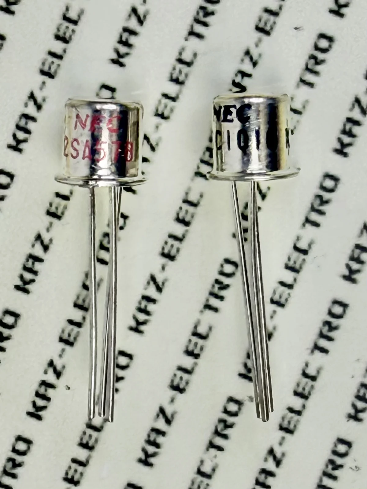
Into the 1970s, NEC introduced low-noise transistors with improved breakdown voltage and current gain through an alumina passivation structure. NEC’s first complementary pair was the 2SA578 (1972) / 2SC1010 (1969), but these were metal-can industrial products, targeting a different market from the general consumer orientation of competing manufacturers.
For consumer use, NEC had the resin-package 2SA640 (45V, 1971), 2SC900 (25V, 1972), and 2SC1222 (50V, 1972) — but with PNP and NPN breakdown voltages and characteristics not well matched, NEC did not designate these as a complementary pair.
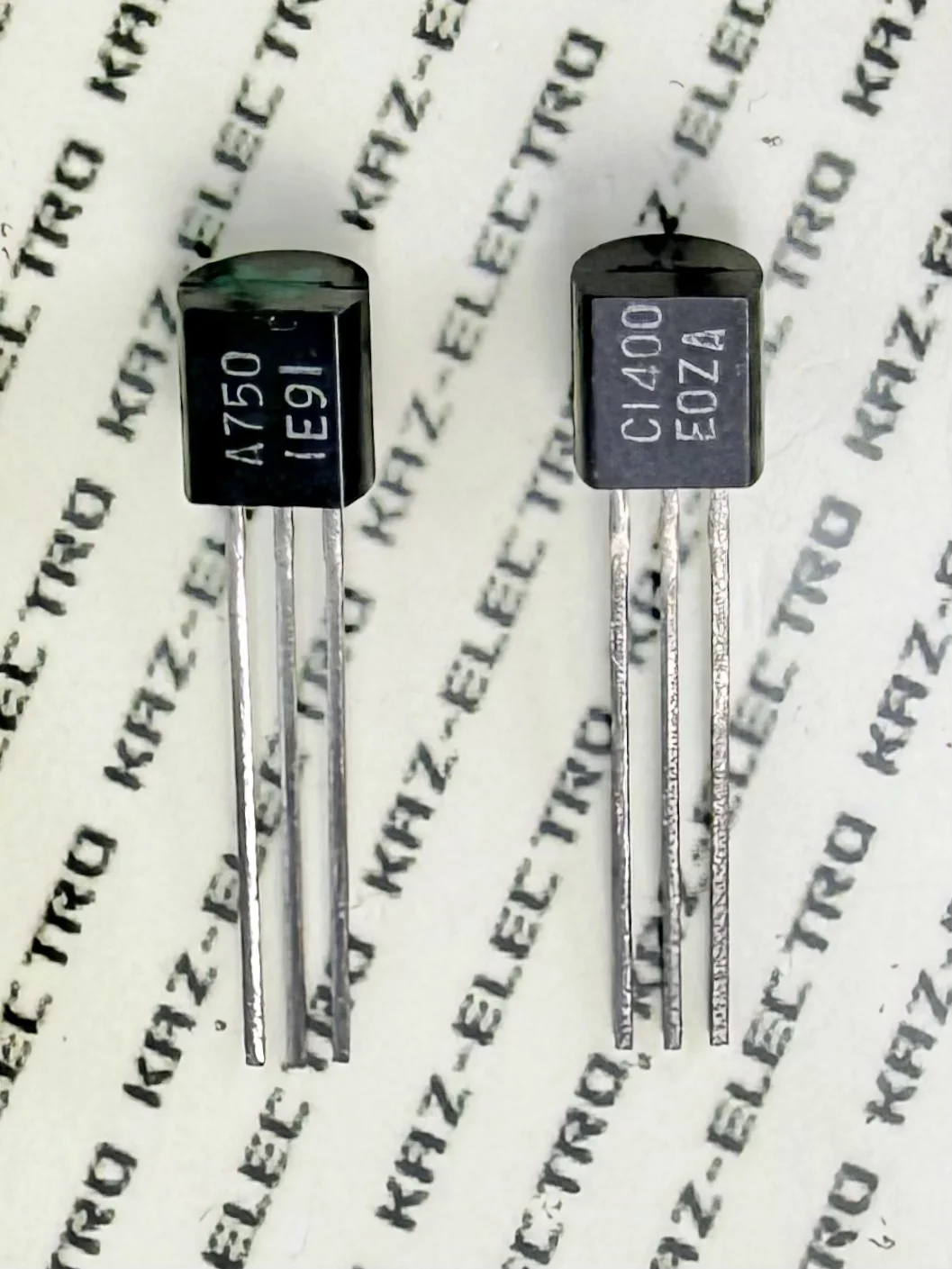
As a result, NEC’s first fully realized 50V-class low-noise complementary pair was the 2SA750/2SC1400 (1973–74), a somewhat later entry than its competitors.
| Package | Type | Vceo | Year | ’65 | ’66 | ’67 | ’68 | ’69 | ’70 | ’71 | ’72 | ’73 | ’74 | ’75 | ’76 | ’77 | ’78 | ’79 |
|---|---|---|---|---|---|---|---|---|---|---|---|---|---|---|---|---|---|---|
| disk | 2SA543﹡ | 25 | 1969 | ﹡ | ﹡ | ﹡ | ﹡ | ﹡ | ﹡ | ﹡ | ﹡ | |||||||
| 2SC475﹡ | 15 | 1968 | ﹡ | ﹡ | ﹡ | ﹡ | ﹡ | ﹡ | ﹡ | ﹡ | ﹡ | ﹡ | ﹡ | ﹡ | ||||
| TO-72 | 2SA578 | 40 | 1972 | ■ | ■ | ■ | ■ | ■ | ■ | ■ | ■ | |||||||
| 2SC1010 | 40 | 1969 | ■ | ■ | ■ | ■ | ■ | ■ | ■ | ■ | ■ | ■ | ■ | |||||
| TO-92 | 2SA640﹡ | 45 | 1971 | ﹡ | ﹡ | ﹡ | ﹡ | ﹡ | ﹡ | ﹡ | ﹡ | ﹡ | ||||||
| 2SC900﹡ | 25 | 1972 | ﹡ | ﹡ | ﹡ | ﹡ | ﹡ | ﹡ | ﹡ | ﹡ | ||||||||
| 2SC1222﹡ | 50 | 1972 | ﹡ | ﹡ | ﹡ | ﹡ | ﹡ | ﹡ | ﹡ | ﹡ | ||||||||
| TO-92 | 2SA750 | 50 | 1973 | ■ | ■ | ■ | ■ | ■ | ■ | ■ | ||||||||
| 2SC1400 | 50 | 1974 | ■ | ■ | ■ | ■ | ■ | ■ |
Source: Transistor Specifications Reference (CQ Publishing), various years; Transistor Compatibility Reference (CQ Publishing), various years; NEC Semiconductor Databook, various years
Matsushita
Matsushita’s first low-noise transistor was the 2SC539 (1970), a metal-can packaged device. The following year, 1971, saw the resin-package 2SA666 (25V), 2SA666A (45V), and 2SC644 (25V) — making Matsushita one of the early movers in bringing low-noise transistors to the consumer market. However, no 45V-class product existed on the NPN side, and Matsushita itself did not position the 2SA666 and 2SC644 as a complementary pair.
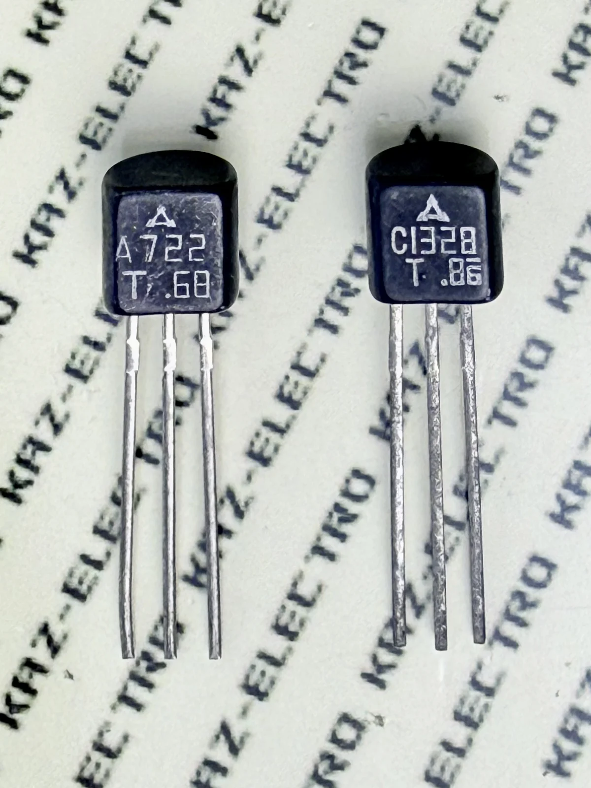
The first official complementary pair appeared in 1973. That year, two voltage-variant siblings debuted simultaneously: the 2SA721/2SC1327 (35V) and 2SA722/2SC1328 (55V). The latter’s 55V class (2SA722/2SC1328) achieved a 5V higher breakdown voltage than competing products of the same period — a notably superior specification.
| Package | Type | Vceo | Year | ’65 | ’66 | ’67 | ’68 | ’69 | ’70 | ’71 | ’72 | ’73 | ’74 | ’75 | ’76 | ’77 | ’78 | ’79 |
|---|---|---|---|---|---|---|---|---|---|---|---|---|---|---|---|---|---|---|
| TO-72 | 2SC539﹡ | 25 | 1970 | ﹡ | ﹡ | ﹡ | ﹡ | ﹡ | ﹡ | ﹡ | ﹡ | ﹡ | ﹡ | |||||
| TO-92 | 2SA666﹡ | 25 | 1971 | ﹡ | ﹡ | ﹡ | ﹡ | ﹡ | ﹡ | ﹡ | ﹡ | ﹡ | ||||||
| 2SA666A﹡ | 45 | 1971 | ﹡ | ﹡ | ﹡ | ﹡ | ﹡ | ﹡ | ﹡ | ﹡ | ﹡ | |||||||
| 2SC644﹡ | 25 | 1971 | ﹡ | ﹡ | ﹡ | ﹡ | ﹡ | ﹡ | ﹡ | ﹡ | ﹡ | |||||||
| TO-92 | 2SA721 | 35 | 1973 | ■ | ■ | ■ | ■ | ■ | ■ | ■ | ||||||||
| 2SC1327 | 35 | 1972 | ■ | ■ | ■ | ■ | ■ | ■ | ■ | ■ | ||||||||
| TO-92 | 2SA722 | 55 | 1973 | ■ | ■ | ■ | ■ | ■ | ■ | ■ | ||||||||
| 2SC1328 | 55 | 1972 | ■ | ■ | ■ | ■ | ■ | ■ | ■ | ■ |
Source: Transistor Specifications Reference (CQ Publishing), various years; Transistor Compatibility Reference (CQ Publishing), various years; Matsushita Electronics Databook, various years
Hitachi
Hitachi appears to have released low-noise transistors, the 2SA567/2SC649, around 1968–70. These had a classic appearance reminiscent of the TO-1 package from the germanium era, but disappeared almost as soon as they appeared; details are unclear.
The device most properly regarded as the first serious low-noise transistor from Hitachi was the 2SC458LG (1969) — a low-noise grade of the 1965 2SC458, employing Hitachi’s proprietary LTP (Low Temperature Passivation) technology.
In 1972, Hitachi also released the 50V-class low-noise transistors 2SA672 and 2SC1345, but did not designate them as a complementary pair. In 1977, the 2SA672 was replaced by the 2SA836 — which also had similar ratings and characteristics to the 2SC1345, but again without a complementary designation.
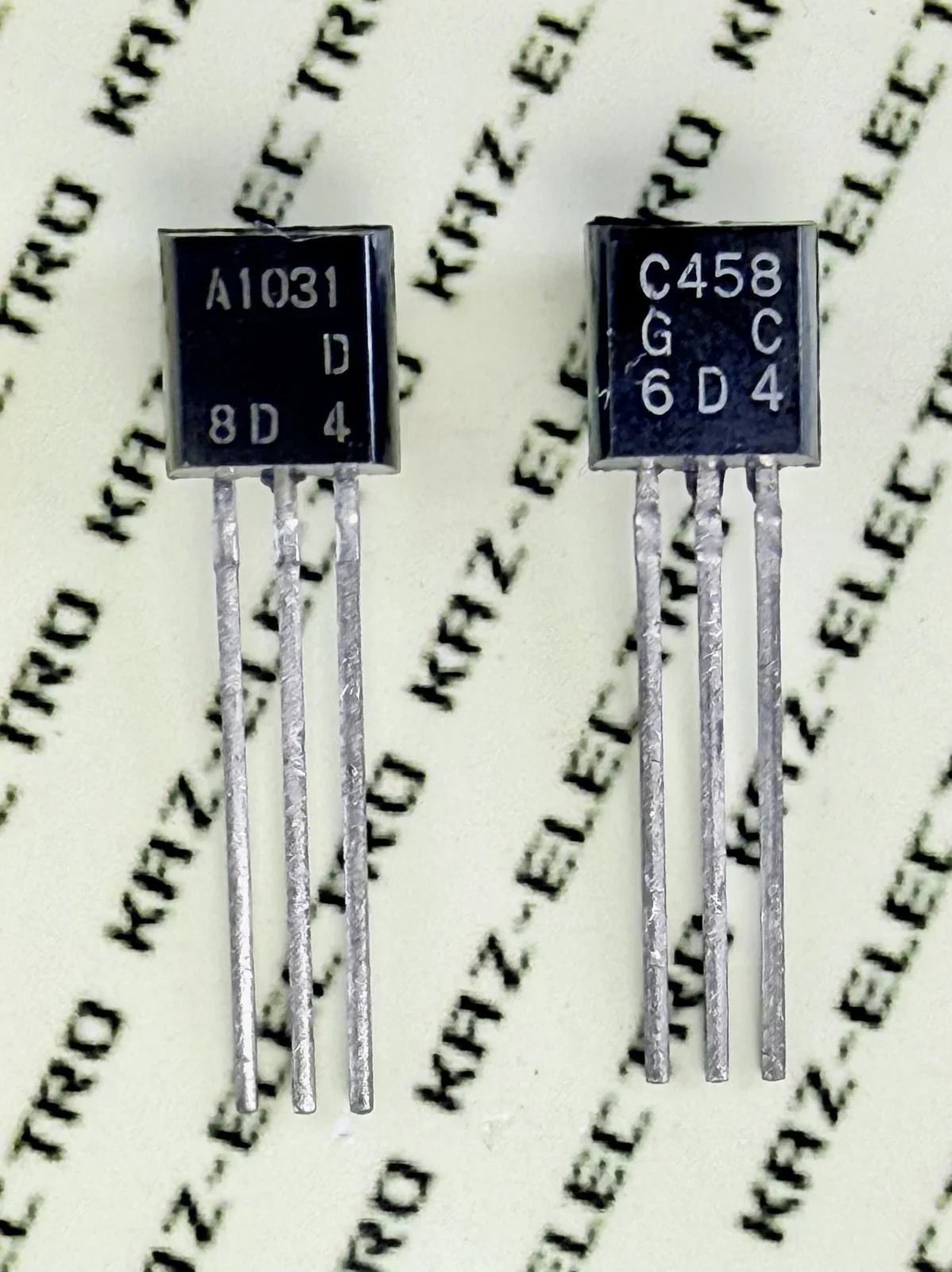
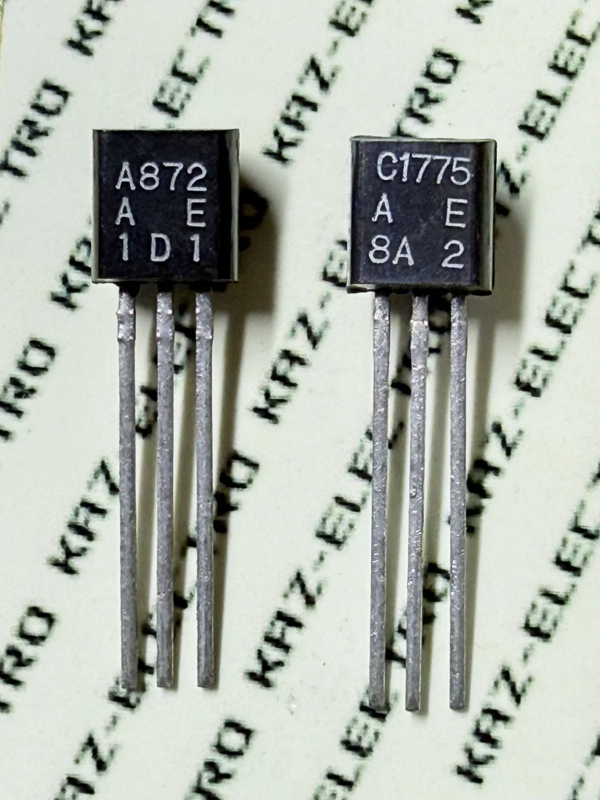
Hitachi’s first low-noise complementary pair was therefore the 2SA872/2SC1775, appearing in 1977. Meanwhile, the 2SC458LG — low-voltage at VCEO = 30V as its name suggests — reigned as the standard for low-noise NPN. Such was its popularity that a complementary PNP, the 2SA1031, was added ten years later in 1979 — an unusual development. (The author infers that “LG” stands for Low-noise Grade.)
| Package | Type | Vceo | Year | ’65 | ’66 | ’67 | ’68 | ’69 | ’70 | ’71 | ’72 | ’73 | ’74 | ’75 | ’76 | ’77 | ’78 | ’79 |
|---|---|---|---|---|---|---|---|---|---|---|---|---|---|---|---|---|---|---|
| TO-1 | 2SA567﹡ | 30 | 1970 | ﹡ | ||||||||||||||
| 2SC649﹡ | 25 | 1968 | ﹡ | ﹡ | ﹡ | |||||||||||||
| proprietary/TO-92 | 2SA1031 | 30 | 1979 | ■ | ||||||||||||||
| 2SC458LG | 30 | 1969 | ■ | ■ | ■ | ■ | ■ | ■ | ■ | ■ | ■ | ■ | ■ | |||||
| proprietary | 2SA672﹡ | 50 | 1972 | ﹡ | ﹡ | ﹡ | ﹡ | ﹡ | ||||||||||
| 2SA836﹡ | 55 | 1977 | ﹡ | ﹡ | ﹡ | |||||||||||||
| 2SC1345﹡ | 50 | 1972 | ﹡ | ﹡ | ﹡ | ﹡ | ﹡ | ﹡ | ﹡ | ﹡ | ||||||||
| TO-92 | 2SA872 | 90 | 1977 | ■ | ■ | ■ | ||||||||||||
| 2SC1775 | 90 | 1977 | ■ | ■ | ■ |
Source: Transistor Specifications Reference (CQ Publishing), various years; Transistor Compatibility Reference (CQ Publishing), various years; Hitachi Semiconductor Databook, various years
Sanyo
Sanyo released the 2SC693 and 2SC694 (both 30V) in 1970, and the 2SA701 (30V) and 2SA702 (50V) in 1972 — but these early low-noise products were not complementary pairs and had disappeared from the market by the mid-1970s.
The first 50V complementary pair from Sanyo was the 2SA929/2SC1570, but its 1978 debut was the latest of any major manufacturer. During the 1970s, Sanyo appears to have focused more on low-voltage products for radios and tape recorders, and on television products, rather than on complementary pairs for hi-fi audio.
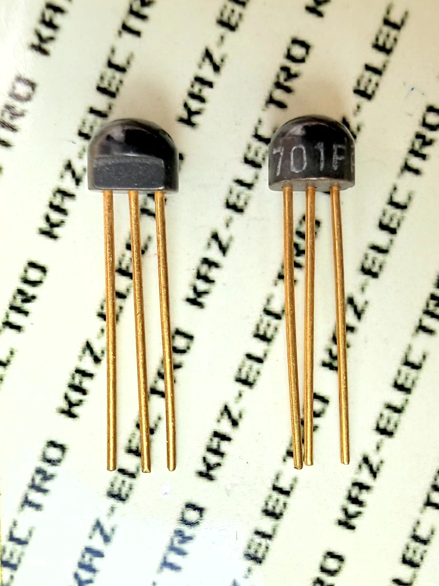
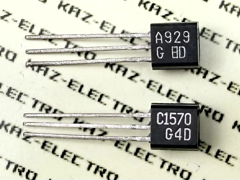
| Package | Type | Vceo | Year | ’65 | ’66 | ’67 | ’68 | ’69 | ’70 | ’71 | ’72 | ’73 | ’74 | ’75 | ’76 | ’77 | ’78 | ’79 |
|---|---|---|---|---|---|---|---|---|---|---|---|---|---|---|---|---|---|---|
| proprietary | 2SA701﹡ | 30 | 1972 | ﹡ | ﹡ | ﹡ | ﹡ | ﹡ | ﹡ | ﹡ | ﹡ | |||||||
| 2SA702﹡ | 50 | 1972 | ﹡ | ﹡ | ﹡ | ﹡ | ﹡ | ﹡ | ﹡ | ﹡ | ||||||||
| 2SC693﹡ | 30 | 1970 | ﹡ | ﹡ | ﹡ | ﹡ | ﹡ | ﹡ | ﹡ | ﹡ | ﹡ | ﹡ | ||||||
| 2SC694﹡ | 30 | 1970 | ﹡ | ﹡ | ﹡ | ﹡ | ﹡ | ﹡ | ﹡ | ﹡ | ||||||||
| TO-92 | 2SA929 | 50 | 1978 | ■ | ■ | |||||||||||||
| 2SC1570 | 50 | 1978 | ■ | ■ |
Source: Transistor Specifications Reference (CQ Publishing), various years; Transistor Compatibility Reference (CQ Publishing), various years; Sanyo Semiconductor Databook, various years
Mitsubishi
Mitsubishi introduced low-voltage NPN low-noise transistors in 1972 — the 2SC1312 (35V) and 2SC1313 (50V). The following year, 1973, the PNP counterparts 2SA725 (35V) and 2SA726 (50V) followed — but with subtle differences between NPN and PNP in maximum ratings and characteristics, Mitsubishi refrained from designating them as a complementary pair.
Subsequently, further low-noise PNP and NPN devices were released in pairs, but declining to designate them as complementary remained Mitsubishi’s characteristic approach.
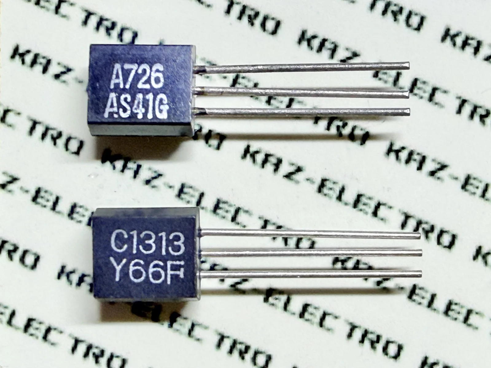
| Package | Type | Vceo | Year | ’65 | ’66 | ’67 | ’68 | ’69 | ’70 | ’71 | ’72 | ’73 | ’74 | ’75 | ’76 | ’77 | ’78 | ’79 |
|---|---|---|---|---|---|---|---|---|---|---|---|---|---|---|---|---|---|---|
| TO-92 | 2SA725﹡ | 35 | 1973 | ﹡ | ﹡ | ﹡ | ﹡ | ﹡ | ﹡ | ﹡ | ||||||||
| 2SC1312﹡ | 35 | 1972 | ﹡ | ﹡ | ﹡ | ﹡ | ﹡ | ﹡ | ﹡ | ﹡ | ||||||||
| TO-92 | 2SA726﹡ | 50 | 1973 | ﹡ | ﹡ | ﹡ | ﹡ | ﹡ | ﹡ | ﹡ | ||||||||
| 2SC1313﹡ | 50 | 1972 | ﹡ | ﹡ | ﹡ | ﹡ | ﹡ | ﹡ | ﹡ | ﹡ |
Source: Transistor Specifications Reference (CQ Publishing), various years; Transistor Compatibility Reference (CQ Publishing), various years; Mitsubishi Semiconductor Databook, various years
Sony
Sony manufactured transistors primarily for use in its own products. It released complementary pairs with different voltage variants: the 2SA704/2SC631A (25V) and 2SA705/2SC632A (50V). In both cases the NPN appeared in 1971, while the PNP was delayed until 1973 — a situation similar to contemporaries at other manufacturers.
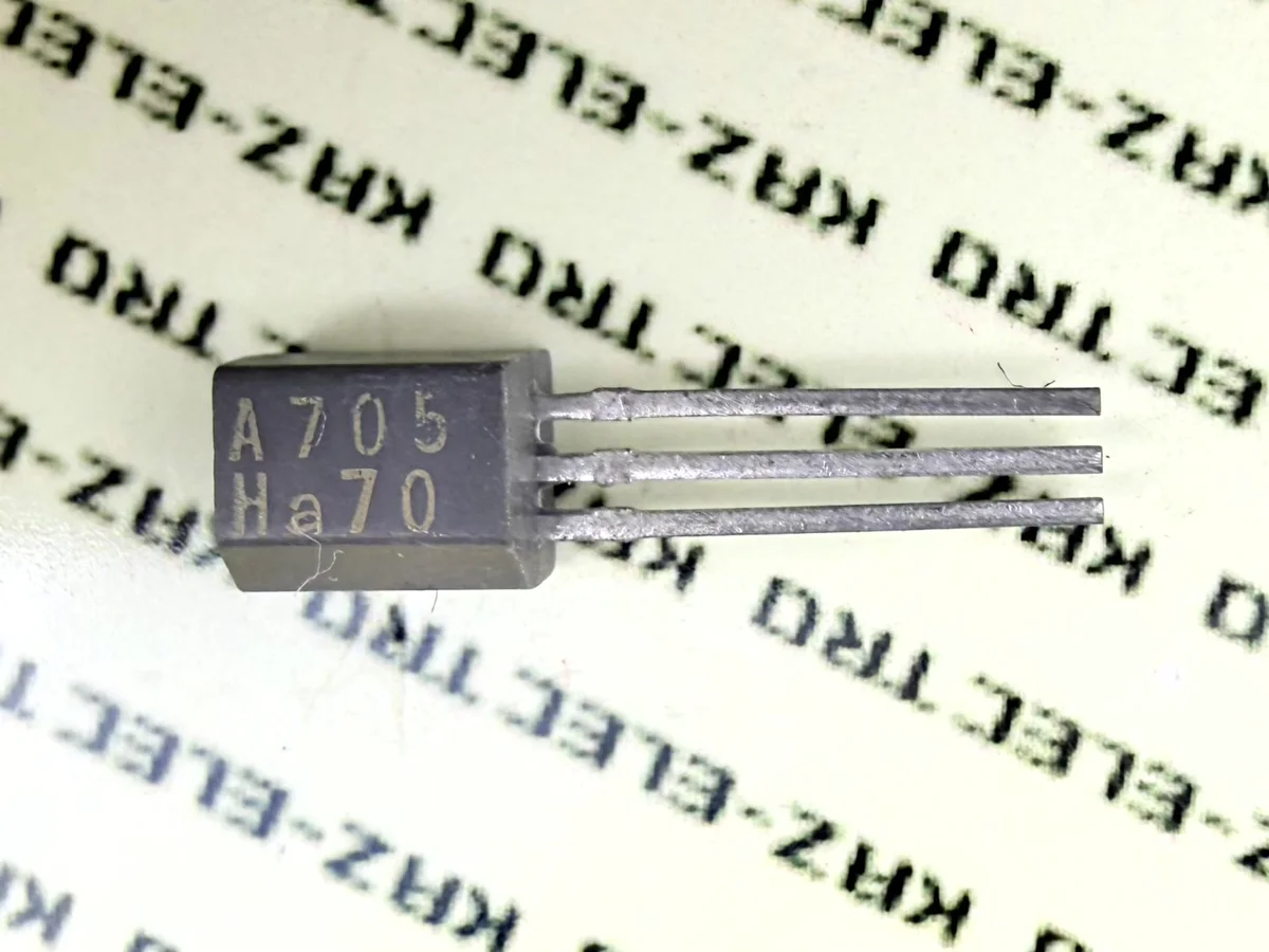
| Package | Type | Vceo | Year | ’65 | ’66 | ’67 | ’68 | ’69 | ’70 | ’71 | ’72 | ’73 | ’74 | ’75 | ’76 | ’77 | ’78 | ’79 |
|---|---|---|---|---|---|---|---|---|---|---|---|---|---|---|---|---|---|---|
| proprietary | 2SA704 | 25 | 1973 | ■ | ■ | ■ | ■ | ■ | ■ | ■ | ||||||||
| 2SC631A | 25 | 1971 | ■ | ■ | ■ | ■ | ■ | ■ | ■ | ■ | ■ | |||||||
| proprietary | 2SA705 | 50 | 1973 | ■ | ■ | ■ | ■ | ■ | ■ | ■ | ||||||||
| 2SC632A | 50 | 1971 | ■ | ■ | ■ | ■ | ■ | ■ | ■ | ■ | ■ |
Source: Transistor Specifications Reference (CQ Publishing), various years; Transistor Compatibility Reference (CQ Publishing), various years; Sony Databook, various years
Section 8.1 Summary
Toshiba, which had led the market in low-cost resin-encapsulated transistors and silicon complementary pairs for audio, also led in low-noise transistor development. The 2SA493/2SC1000, appearing in 1971, was relaunched around 1980 as the 2SA493GTM/2SC1000GTM and maintained the family’s lineage for approximately 20 years, into the early 1990s.
Overall tendencies:
- PNP tended to appear later than NPN across all manufacturers.
- Each manufacturer’s 50V low-noise complementary pair came together around 1973.
8.2 “The Four Technical Hurdles” in Low-Noise PNP Development
At the time, achieving “low noise,” “high breakdown voltage,” “PNP,” and “resin package” simultaneously represented a challenge where the physical and chemical difficulties confronting semiconductor technology converged all at once.
1. Difficulties inherent to silicon PNP devices
- Hole mobility is lower in PNP, placing it at a disadvantage in high-frequency characteristics and drive capability compared to NPN
- Positive charges accumulate easily at the SiO₂ interface, making parasitic channels (channeling effect) more prone to occur
- This is a primary cause of increased leakage current and reduced breakdown voltage
2. The barrier of high breakdown voltage
- Securing high Vceo in PNP is particularly difficult
- Epitaxial layer control is harder, and the ASO (Area of Safe Operation) tends to be narrower than for NPN
- Secondary breakdown suppression technology — preventing instantaneous failure in regions where high voltage and high current coincide — was immature
3. Technical challenges of low-cost resin packaging
- Unlike metal cans, resin is non-hermetic, allowing moisture to penetrate to the die surface
- Thermal expansion differences between resin and silicon cause interfacial delamination
- This increases surface state density, becoming a cause of leakage current and popcorn noise
4. The barrier of low-noise performance and pair matching
- The key to low-noise performance is suppression of 1/f noise
- This depends strongly on surface state density — a chemically delicate process for PNP, placing it at a disadvantage relative to NPN
- Low yields in hFE and Vbe matching essential for audio applications also posed a barrier to volume production
In the 1960s–70s, manufacturers competed to develop low-noise complementary pairs. Toshiba achieved Japan’s first low-noise complementary pair with the 2SA494G/2SC369G (30V class, 1970), following it the next year with the high-voltage 2SA493/2SC1000 (50V class). The 50V low-noise complementary pairs of each major manufacturer came together around 1973.
As an overall tendency, PNP tended to appear later than NPN. This was a consequence of The Four Technical Hurdles: the hFE barrier inherent to PNP, the tension between high breakdown voltage and low noise, the tension between resin encapsulation and low noise, and the barrier to pair matching. Toshiba’s ability to lead the market in low-cost resin-encapsulated transistors and complementary pairs was possible precisely because of its overcoming of The Four Technical Hurdles through PCT technology.
→ Next chapter: An examination of how the 2SA493/2SC1000 family was documented in Toshiba databooks, and how that documentation evolved.
9. Twenty Years in Print — A History Through the Databooks
The 2SA493/2SC1000 family had a product life of roughly twenty years, though the exact date of final production remains unclear. Adding to the puzzle, the 2SA493 (standard, no suffix) disappeared from the NRND/DISCON product lists in Toshiba’s own databooks for reasons that remain unclear — and stayed missing. In this chapter, the author traces the family’s entire life span through Toshiba’s official publications, from the first databook appearance in 1973 through a final SMD catalogue reference in 2005, examining the record from multiple angles.
9.1 First Official Listing: The 2SA493/2SC1000 and G Series (1973)
The 2SA493/2SC1000 made its first official databook appearance in the Toshiba Semiconductor Handbook 1973 (Toshiba, published November 1972). It was not listed in the 1971 edition (published 1970), though market supply is estimated to have begun around 1971 (see Section 7.1.1).
9.2 PCT Technology: From Technical Completion to Full Promotion (1969–1975)
The 2SA493/2SC1000 uses Toshiba’s PCT method (Perfect Crystal device Technology), completed in 1969. It should be noted, however, that PCT is more accurately described as an incremental refinement built on top of existing planar technology — a layered improvement, not a prerequisite — rather than the foundation that made low-noise performance possible. The 2SC369, a low-noise device that can be regarded as an ancestor of the 2SC1000, had already appeared in 1965, well before PCT existed. A 2SC1000 unit estimated to date from 1969 has also been confirmed in the author’s collection.
What Is PCT? (From the Toshiba Databook, 1975)
Background
Transistor technology advanced through three major developments: the shift from germanium to silicon, surface stabilization techniques, and improvements to resin packaging. Surface stabilization was generally referred to as “planar” technology. In 1969, Toshiba completed and commercialized its proprietary process, which it named Perfect Crystal device Technology.
Technical Definition
- Abbreviation of: Perfect Crystal device Technology
- Uses wafer material that is a perfect crystal, free of dislocations and other defects
- Manufacturing steps — epitaxial growth, diffusion, oxidation — are carried out without introducing new defects
- Maintains perfect crystal condition throughout the fabrication of the finished semiconductor device
Characteristics of PCT Transistors
- Low noise: Low-frequency noise is reduced because crystal strain is absent
- Improved high-frequency characteristics: In conventional diffusion processes, dislocation spreading into the base region during emitter diffusion — the “emitter dip effect” — degraded high-frequency performance. PCT corrects this.
- High carrier lifetime: Absence of crystal defects extends carrier lifetime, contributing to improved linearity and reduced saturation voltage in power transistors
In the 1960s, “planar technology” was a broad term covering surface stabilization by silicon dioxide passivation. PCT was a further development of that concept. Until around 1973, however, it appeared only modestly, in the technical notes section of individual datasheets, and whether PCT was applied to any given device was not disclosed.
From 1975 onward, Toshiba began foregrounding PCT prominently — describing its products as “Silicon Epitaxial Transistors (PCT process)” and emphasizing it as a proprietary technology rather than the generic word “planar.” This shift accompanied both the stabilization of the manufacturing process and improvements in yield, and it appears to reflect a strengthening of marketing strategy alongside those technical gains. That the mass production rollout of PCT itself required considerable time is apparent. Whether it was a direct cause of the delay in the 2SA493/2SC1000’s market debut, however, the author cannot say definitively.
9.3 The Short Life of the 2SA493 — and the Survival of the 2SA493G (1976)
The 2SA493, having established itself in the market as a pioneer among 50V-class low-noise complementary pairs, was designated NRND in 1976 — ahead of its companion 2SC1000.
Successors 2SA841/2SC1681 and 2SA842/2SC1682 stepped in, and in formal terms, the 2SA493 passed the baton after barely five years. Demand proved persistent, however, and production continued in NRND status until approximately 1980.
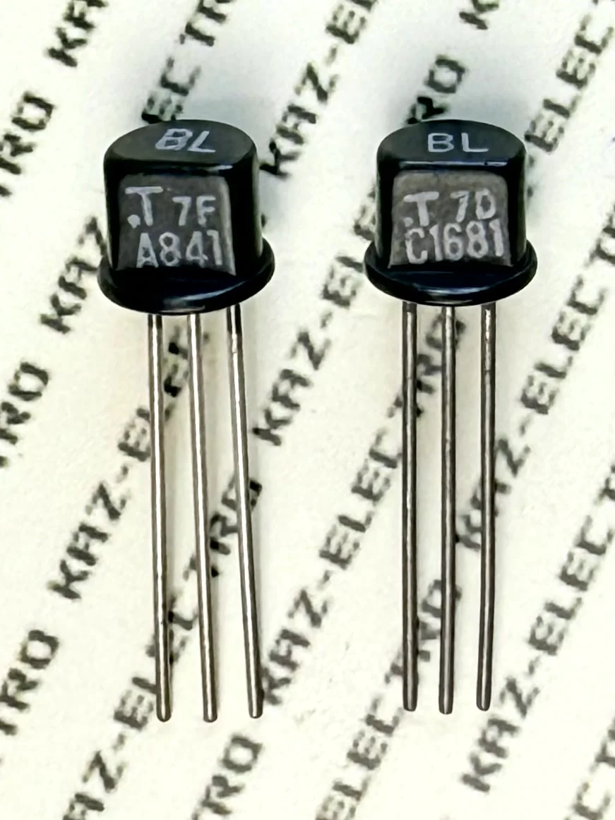
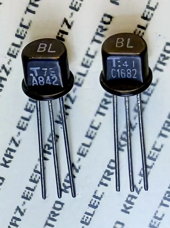
The Green Series 2SA493G/2SC1000G, meanwhile, remained in active production. Why only the standard 2SA493 was designated NRND so early is discussed in detail in Section 6.4, “Does the 2SA493TM Exist?”
The surviving 2SA493G received the benefit of Toshiba’s most current process at the time, and a new high-hFE rank — “BL” — was added. PNP transistors are structurally prone to lower hFE and difficult to produce in volume at high hFE levels. Toshiba overcame this, achieving volume production of high-hFE PNP devices.
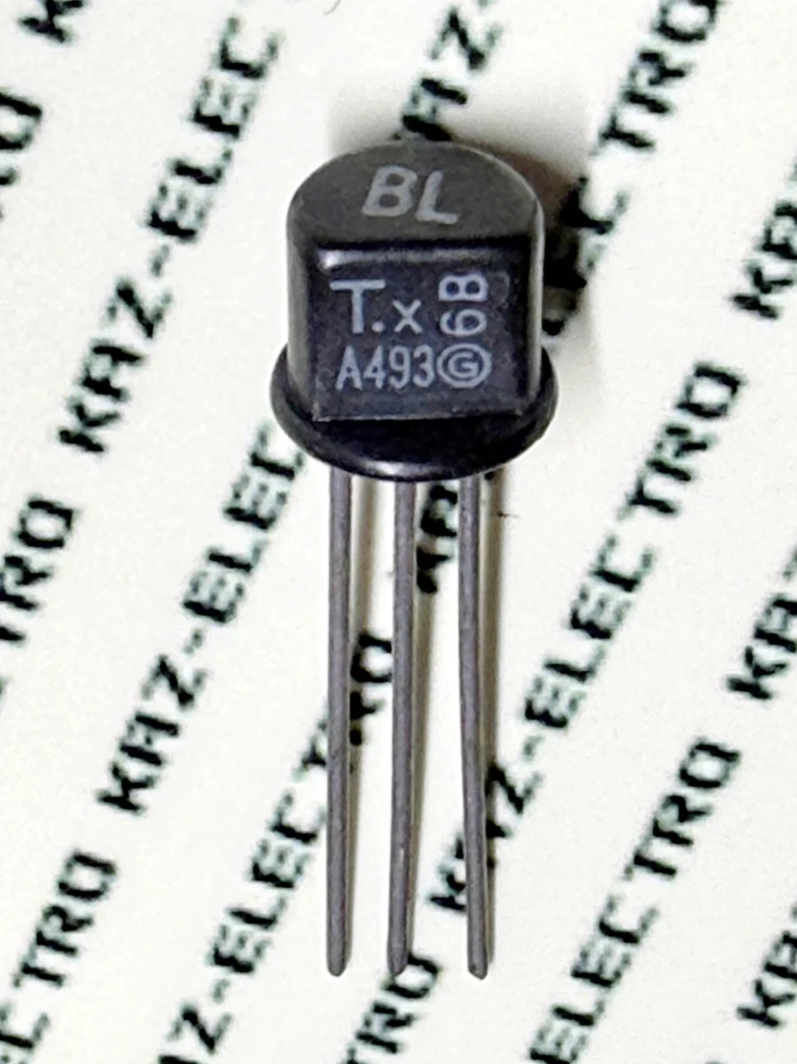
The result was a meaningful advance: where the 2SA493G/2SC1000G had previously been matchable only at the GR rank, the pair could now be complementary-matched at the BL rank as well.
9.3.1 How Was It Overcome?
This was the result of broad advances across semiconductor manufacturing technology:
- Maturation of double-diffusion techniques
- Higher precision photolithography → enabled extreme narrowing of the PNP base width
- Improvements in epitaxial layer quality
- Spread of ion implantation technology
- Evolution of surface passivation techniques
These developments, taken together, enabled the high hFE that was previously out of reach.
9.4 Tracing the Successor Designations in Toshiba’s Databooks
In Toshiba’s databooks, products designated NRND (Not Recommended for New Design) or DISCON (Discontinued) are listed alongside recommended successor devices. For the 2SA493/2SC1000 family, however, those successor designations shifted in complex ways across editions — and the picture does not resolve cleanly.
The author surveyed sixteen Toshiba official publications spanning 1966 to 2005, tracking the listing status and successor changes for each device. This section begins with an overview of the full trajectory, then examines the individual anomalies, before presenting the complete data as a reference table.
9.4.1 Overview of the Product Life Cycle
The 2SA493/2SC1000 family’s product life cycle divides broadly into five periods.
| Period | Standard (2SA493/2SC1000) |
G Series (2SA493G/2SC1000G) |
GTM Series (2SA493GTM/2SC1000GTM) |
|---|---|---|---|
| 1971–1975 Peak years |
Active | Active (from 1973) | — |
| 1976–1979 Standard goes NRND |
NRND Successor: 2SA842 → 2SA970 |
Active → NRND | — |
| 1980–1982 GTM launches, generational handoff |
NRND | NRND Successor: GTM |
Active |
| 1983–1988 Standard and G go DISCON |
DISCON ※ missing from list |
DISCON Successor: GTM |
Active |
| 1988–1990 GTM goes NRND → DISCON |
— | DISCON Successor: 2SA1015 |
DISCON Successor: 2SA970 / 2SA1015 (varies) |
Within this trajectory, several anomalies surface. Each is examined below.
9.4.2 The Unexplained Disappearance of the 2SA493 (Standard)
From 1983 onward, the 2SA493 (standard, no suffix) alone is consistently missing from the NRND/DISCON product lists in every Toshiba databook the author has examined. The standard 2SC1000, and the variants 2SA493G and 2SA493GTM, are all listed — only the 2SA493 is absent.
Across every Toshiba databook examined — five separate publications spanning 1983 to 2005 — the 2SA493 (standard) does not appear in the NRND/DISCON product list. An absence of more than twenty years. Whether this represents a simple editorial omission or something more deliberate, the author cannot determine.
9.4.3 Asymmetry in Successor Designations
On the NPN side, the 2SC2240 is designated consistently as the successor for the standard, G, GTM, and TM variants alike. On the PNP side, by contrast, the successor designations vary across publications, presenting a strikingly different picture.
- 2SA493 (standard): 2SA842 → 2SA970 (then missing from list entirely)
- 2SA493G: 2SA493GTM → 2SA1015 (general-purpose device)
- 2SA493GTM: fluctuates between 2SA970 and 2SA1015 depending on edition
Tracing the 2SA493GTM’s successor designations in chronological order makes the extent of the variation clear:
- 1988 edition (Small-Signal Transistors): 2SA1015 ★ earliest recorded successor designation
- 1990 edition (Power Transistor Databook): 2SA970
- 1999 edition (Power Transistor Databook): 2SA1015
- 2005 edition (Small-Signal Transistors SMD): 2SA970
The 2SA970 is a legitimate low-noise transistor and a natural successor to the 2SA493GTM. The 2SA1015, by contrast, is a general-purpose small-signal transistor, not primarily positioned for low-noise applications. Why the latter was designated as a successor at all is a question the databooks leave unanswered — though one clue exists.
The 2SA1015/2SC1815 datasheet carries the notation: “Noise voltage is controlled: NF = 1 dB (typ.) (f = 1 kHz).” The device is not positioned as a low-noise transistor per se, but it appears Toshiba may have judged that the 2SA1015 was adequate in practical terms as a successor to the 2SA493GTM — by then an older-generation low-noise device.
On the NPN side, the 2SC1000GTM would have enjoyed substantially higher demand than the PNP. The fact that 2SC2240 — the more stringently low-noise option — was designated consistently as its successor suggests a conservative choice. In the author’s reading, this asymmetry in NPN vs. PNP demand may help explain why the PNP successor designations drifted.
One further note: the 2SC1000TM, which was never listed in any databook as an active product, does appear in the NRND/DISCON product lists, with 2SC2240 designated as its successor. The background of the 2SC1000TM is discussed in detail in Chapter 6.
9.4.4 Complete Listing Data
The following table presents the listing status of the 2SA493/2SC1000 family across all sixteen Toshiba publications examined by the author. It is offered as an archival record for future researchers and collectors.
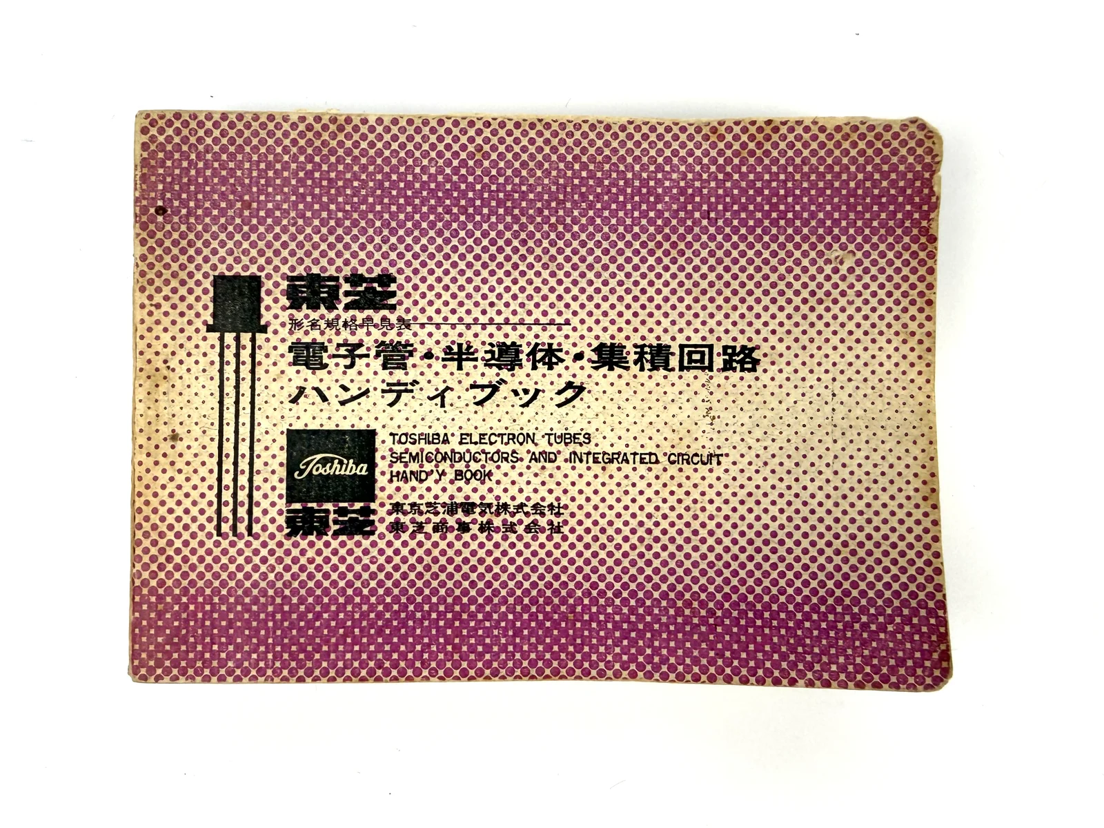
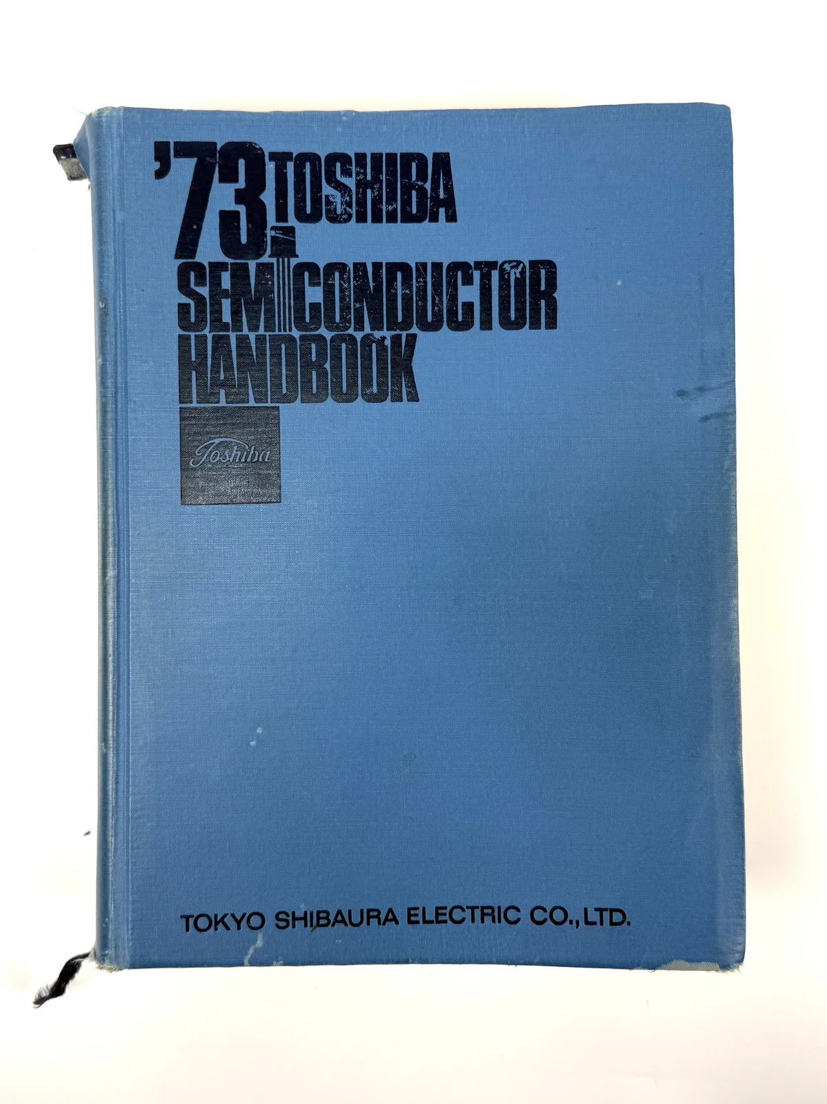
| Publication | Year | 2SA493 | 2SC1000 | 2SA493G | 2SC1000G | 2SA493GTM | 2SC1000GTM | 2SC1000TM |
|---|---|---|---|---|---|---|---|---|
| Toshiba Semiconductor Handbook 3 | 1966 | — | — | — | — | — | — | — |
| Toshiba Electron Tubes, Semiconductors & ICs Handy Book | 1967 | — | — | — | — | — | — | — |
| Toshiba Semiconductor Handbook | 1969 | — | — | — | — | — | — | — |
| Toshiba Semiconductor Handbook | 1971 | — | — | — | — | — | — | — |
| Toshiba Electron Tubes, Semiconductors & ICs Handy Book | 1971 | Active | Active | — | — | — | — | — |
| Toshiba Semiconductor Handbook | 1973 | Active | Active | Active | Active | — | — | — |
| Toshiba Semiconductor Handbook | 1975 | Active | Active | Active | Active | — | — | — |
| TOSHIBA SEMICONDUCTOR DATABOOK | 1977 | 2SA842 (NRND 1976.4) |
Active | Active | Active | — | — | — |
| TOSHIBA SEMICONDUCTOR DATABOOK | 1980 | 2SA970 (NRND 1979.10) |
2SC732TM, 2SC2240 (NRND 1979.10) |
2SA493GTM (NRND 1979.10) |
2SC1000GTM (NRND 1979.10) |
Active | Active | — |
| Toshiba Semiconductor Product Catalog | 1982 | — | — | — | — | Active | Active | — |
| Toshiba Semiconductor Databook | 1983 | — (missing from list) |
2SC2240 (DISCON 1983.4) |
2SA493GTM (DISCON 1983.4) |
2SC1000GTM (DISCON 1983.4) |
Active | Active | 2SC2240 (DISCON 1983.4) |
| Toshiba Semiconductor Databook | 1986 | — (missing from list) |
2SC2240 (DISCON) |
2SA493GTM (DISCON) |
2SC1000GTM (DISCON) |
Active | Active | 2SC2240 (DISCON) |
| Toshiba Semiconductor Product Catalog | 1988 | — | — | — | — | — | — | — |
| Toshiba Semiconductor Databook: Small-Signal Transistors | 1988 | — (missing from list) |
2SC2240 (DISCON) |
2SA1015 (DISCON) |
2SC2240 (DISCON) |
2SA1015 (NRND 1988.9) |
2SC2240 (NRND 1988.9) |
2SC2240 (DISCON) |
| Power Transistor Databook | 1990 | — (missing from list) |
2SC2240 (DISCON) |
2SA1015 (DISCON) |
2SC2240 (DISCON) |
2SA970 (DISCON) |
2SC2240 (DISCON) |
2SC2240 (DISCON) |
| Power Transistor Databook | 1999 | — (missing from list) |
2SC2240 (DISCON) |
2SA1015 (DISCON) |
2SC2240 (DISCON) |
2SA1015 (DISCON) |
2SC2240 (DISCON) |
2SC2240 (DISCON) |
| Small-Signal Transistors SMD | 2005 | — (missing from list) |
2SC2240 (DISCON) |
2SA1015 (DISCON) |
2SC2240 (DISCON) |
2SA970 (DISCON) |
2SC2240 (DISCON) |
2SC2240 (DISCON) |
Table Legend
- Active: Product listed in the catalogue section of the publication
- [successor name] (NRND [year.month]): NRND-designated product. Not recommended for new designs but still in production
- [successor name] (DISCON): Discontinued product. Production has ended
- —: Not listed in the publication
- — (missing from list): Anomalous absence — other devices in the same family are listed, but this device alone is missing
Note on “—”: A dash may indicate any of the following:
- Product not yet in existence at that date
- In production but not yet listed in the catalogue
- Active but omitted from catalogue due to impending NRND status
- NRND/DISCON product not included in the NRND/DISCON list
- Publication has no NRND/DISCON list (Toshiba Semiconductor Product Catalog 1982/1988)
In some cases, the applicable condition can be inferred by comparison with adjacent editions. The notation “— (missing from list)” is used exclusively where other devices in the same family appear in the same publication, but a specific device alone is absent.
Sources: Toshiba Semiconductor Handbook 3 1966; Toshiba Electron Tubes, Semiconductors & ICs Handy Book 1967/1971; Toshiba Semiconductor Handbook 1969/1971/1973/1975; TOSHIBA SEMICONDUCTOR DATABOOK 1977/1980; Toshiba Semiconductor Product Catalog 1982/1988; Toshiba Semiconductor Databook 1983/1986; Toshiba Semiconductor Databook: Small-Signal Transistors 1988; Power Transistor Databook 1990/1999; Small-Signal Transistors SMD 2005.
Note: The Toshiba Electron Tubes, Semiconductors & ICs Handy Book (1967 and 1971 editions) is a compact volume — 15 × 10 cm — but runs to approximately 480 pages and 2.5 cm in thickness, placing it closer in character to a sales catalogue than a technical databook. The hFE rank entries in this publication do not always match those in later databooks. In the table above, it is used only to confirm whether a device appears at all; for rank specifics, the later databooks are treated as the authoritative source. The evolution of hFE ranks is discussed separately in Chapter 12.
[Chapter 9 Summary] The 2SA493/2SC1000 received its first official listing in the Toshiba Semiconductor Handbook 1973 (Toshiba, published November 1972). From 1975 onward, Toshiba’s promotion of PCT technology intensified. In 1976, the standard 2SA493 was designated NRND, while the Telecom/Industrial grade 2SA493G remained in active production — and advanced further, with the addition of the high-hFE “BL” rank.
The successor designation history proved complex: the recommended PNP replacement shifted between 2SA1015 and 2SA970 across different editions, the 2SA493 (standard) disappeared from the NRND/DISCON lists from 1983 onward and never reappeared. A survey of sixteen official publications documents the family’s full trajectory from debut to discontinuation.
→ Next chapter: The “rationalization of manufacturing processes” — the sweeping changes to marking, labeling, and package technology that unfolded from the late 1970s through 1981.
10. Rationalization in the Factory — The End of TO-98 and the Shift to TO-92
This chapter examines the wave of “rationalization” that swept through Toshiba’s small-signal transistor manufacturing operations from the late 1970s through 1981, approaching the subject from three angles: the evolution of marking styles, the simplification of printed information, and the transition in packaging technology.
10.1 Introduction: Fifteen Years of TO-98 — and Its End
In the late 1970s, Japan’s semiconductor industry was caught in a wave of rapid automation. The explosive spread of calculators, color televisions, and audio equipment had driven transistor demand to tens of millions of units per month, and the production infrastructure that had served until then was struggling to keep pace.
At Toshiba, this was a period of expanding manufacturing capacity — the semiconductor plant in Ōita had come online in 1970, among other additions. Industry publications of the time confirm that Japan’s semiconductor companies were aggressively advancing automation in their back-end assembly processes.
The Background and Limitations of the TO-98 Package
A brief note on the role of Toshiba’s proprietary TO-98 package, and the problems it presented, is in order here.
The internal structure of TO-98 was closely modeled on metal-can packages such as the TO-18 — a header-and-post construction. The process of mounting a die on a metal base, wire-bonding it, and then covering it with a resin cap that was filled and cured was, in essence, a substitution of resin for the metal cap welding step of the original metal-can process. As a path toward manufacturing automation and simplification, it remained only a partial step.
This “potting process” — in which a transistor die assembly is inserted into the package body and liquid epoxy is then injected and cured — does not achieve the throughput of the transfer molding process used in TO-92 production, where large numbers of devices are formed simultaneously on a continuous strip of metal lead frames. Potting also introduced quality challenges: air bubble entrapment in the resin and shrinkage during curing required careful process control to manage.
Why TO-98 was adopted at all, despite these limitations, was most likely motivated by material cost reduction rather than productivity. Eliminating the expensive metal cap (kovar or equivalent) and the hermetic glass-seal stem that metal-can construction required would have substantially lowered the per-unit material cost. In the author’s reading, TO-98 was a transitional package of the pre-automation era — slower to produce, but cheaper in materials.
Into the Torrent
The TO-98, which had debuted around 1965 with gold-plated leads, followed a gradual path of simplification across roughly fifteen years. But against the explosive demand growth of the late 1970s, its limitations could no longer be managed. By 1978, a torrent of change arrived in rapid succession — simplification of markings, a shift in packaging technology — and the story closed with a full transition to TO-92.
This chapter reads that “age of the torrent” through the evidence left behind in surviving units and contemporary publications.
10.2 The Evolution of Marking Styles
The evolution of top-surface markings described in Chapter 1 is also a record of the long-term rationalization of the TO-98 package.
Long-Term Rationalization (1960s to Mid-1970s)
Early TO-98 production featured the full “TOSHIBA” logotype, hand-applied color dots on the top face for rank identification, and gold-plated leads — a standard of finish that would be unthinkable today. hFE rank was not printed but indicated by a hand-applied color dot on the crown; GR rank, for instance, received a green dot.
By the late 1960s, this had given way to the “T” mark with standard-font printing and solder-plated leads — a cost-reduction step.
Figs. 10-[recap from Ch.1]:
[No.4] Early type (1968) — hand-applied color dot
[No.5] Mid type (1975) — standard font
[No.6] Late type (1976) — narrow font
[No.7] Final type (1978) — top-face printing eliminated
Reproduced from Section 1.3. The progression of top markings directly reflects each stage of rationalization.
Hand-applied color dot
Standard font
Narrow font
Top-face printing eliminated
The Turbulence of the Final Years (Mid-1970s Onward)
From the mid-1970s onward, narrow-font (horizontally compressed) printing began to appear on some devices. Notably, this narrow font is observed only on a subset of the last product group to debut in TO-98 form — the 2SA841/2SC1681 and 2SA842/2SC1682.
Whether the narrow font was a deliberate step in a rationalization program is not something the author can state definitively. In the era before the 1970s, when Toshiba operated smaller factories scattered across multiple sites, marking policies may have varied by facility. That said, given that narrow-font printing appears only in the final phase of TO-98 production — immediately before the transition to single-face printing and then full TM conversion — placing it within the broader rationalization sequence seems the most natural interpretation.
From a technical standpoint, the narrow font offered a practical advantage. On high-speed drum-type marking machines, ink spread was a serious defect risk. The narrow strokes of compressed lettering reduced ink consumption and accelerated drying, enabling faster movement to inspection and packaging after marking. As production lines pushed toward higher speeds, narrow-font printing was, in the author’s view, not simply a cosmetic change but a practical engineering response to those demands.
It is also worth noting that the “mystery TM variants” observed for the 2SA493/2SC1000 family also appear among the 2SA841/2SC1681 and 2SA842/2SC1682. These were devices at the very edge of the TO-98 era — and directly ahead of them came the 2SA970/2SC2240, the true successors. The years 1978 to 1981, as the surviving units in the author’s collection make visible, were the “age of the torrent” in concentrated form.
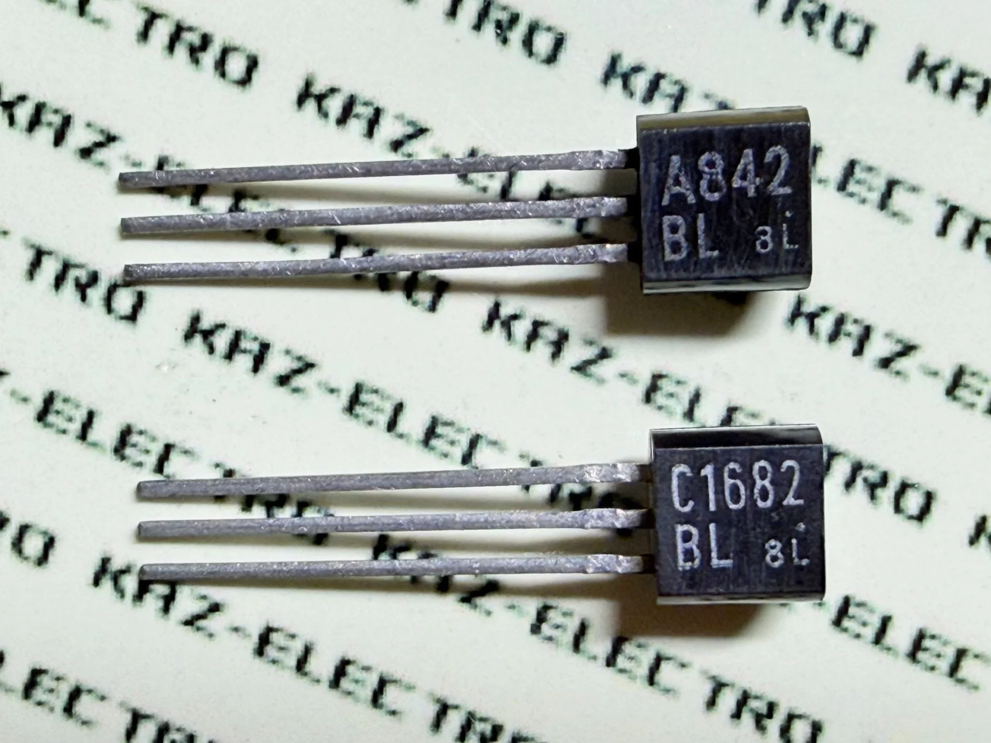
10.3 The Wave of Display Simplification (1978–1980)
TO-98 transistors had featured elaborate two-face printing: hFE rank on the top face, the “T” mark (for Toshiba) with part number on the front face, and lot number on the reverse. From 1978 onward, this was simplified to single-face printing:
- “T” mark eliminated
- hFE rank relocated to lower left of the front face
- Lot number relocated to lower right of the front face
The likely motivation was manufacturing efficiency. Two-face printing required either rotating the package body between passes, or providing multiple print heads for simultaneous printing. Top-face rank marking was a convenience for users — easy to read at a glance — but for the manufacturer it was a time-consuming step. Consolidating all information onto the front face was, in the author’s reading, a rationalization of print cycle time (takt time).
The top face of a TO-98 unit has no parting line from mold forming, making it structurally suited for secondary marking. But as demand surged and throughput became the priority, even this step became a target for elimination.
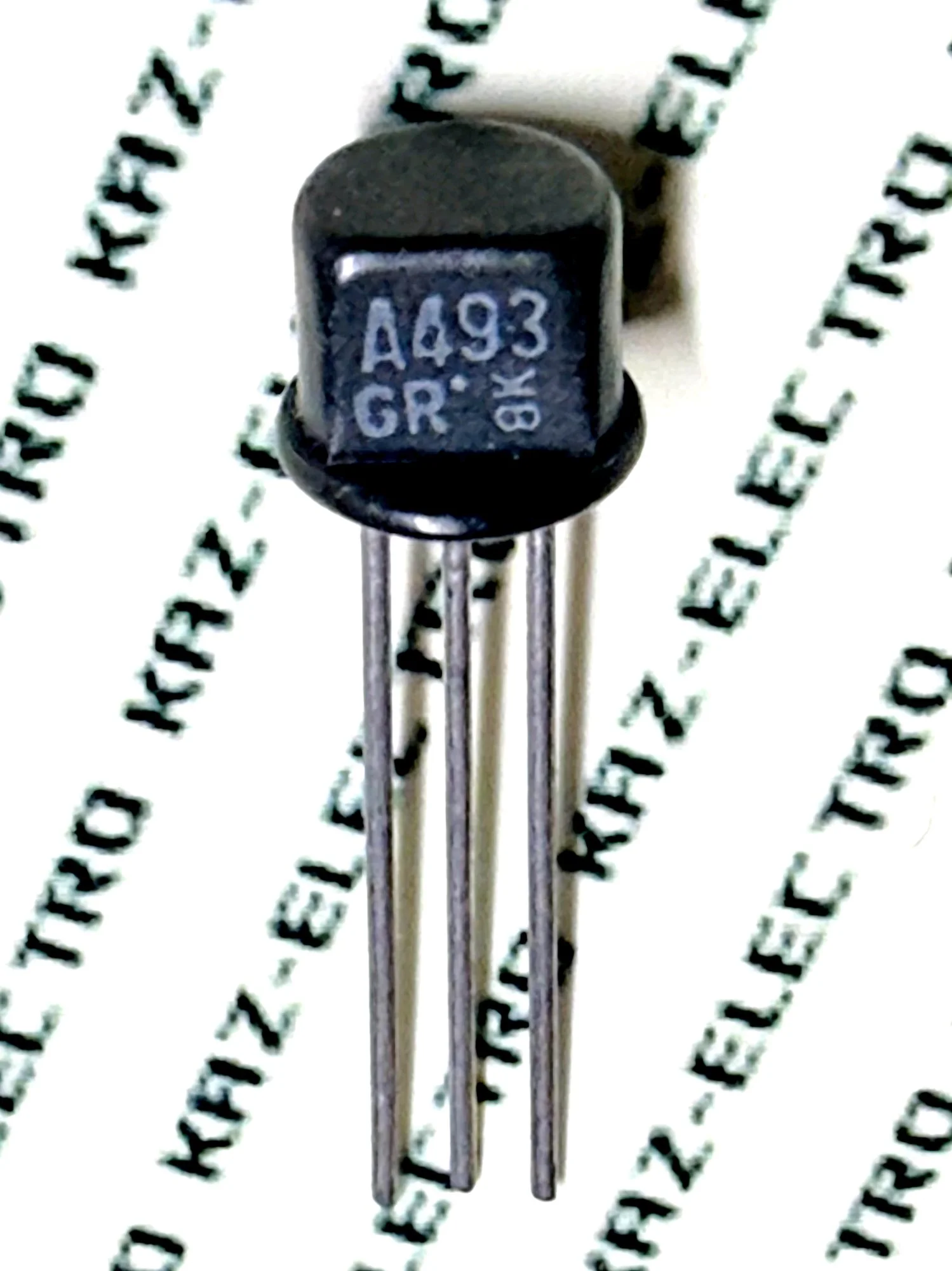
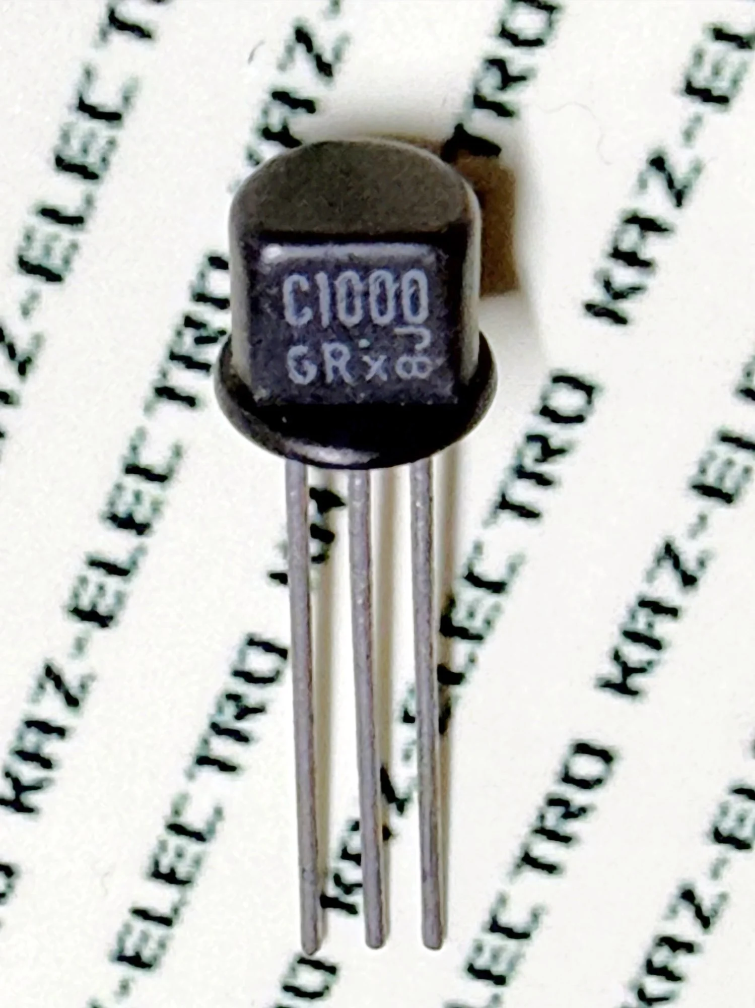
10.4 Observations on “X”-Marked Units
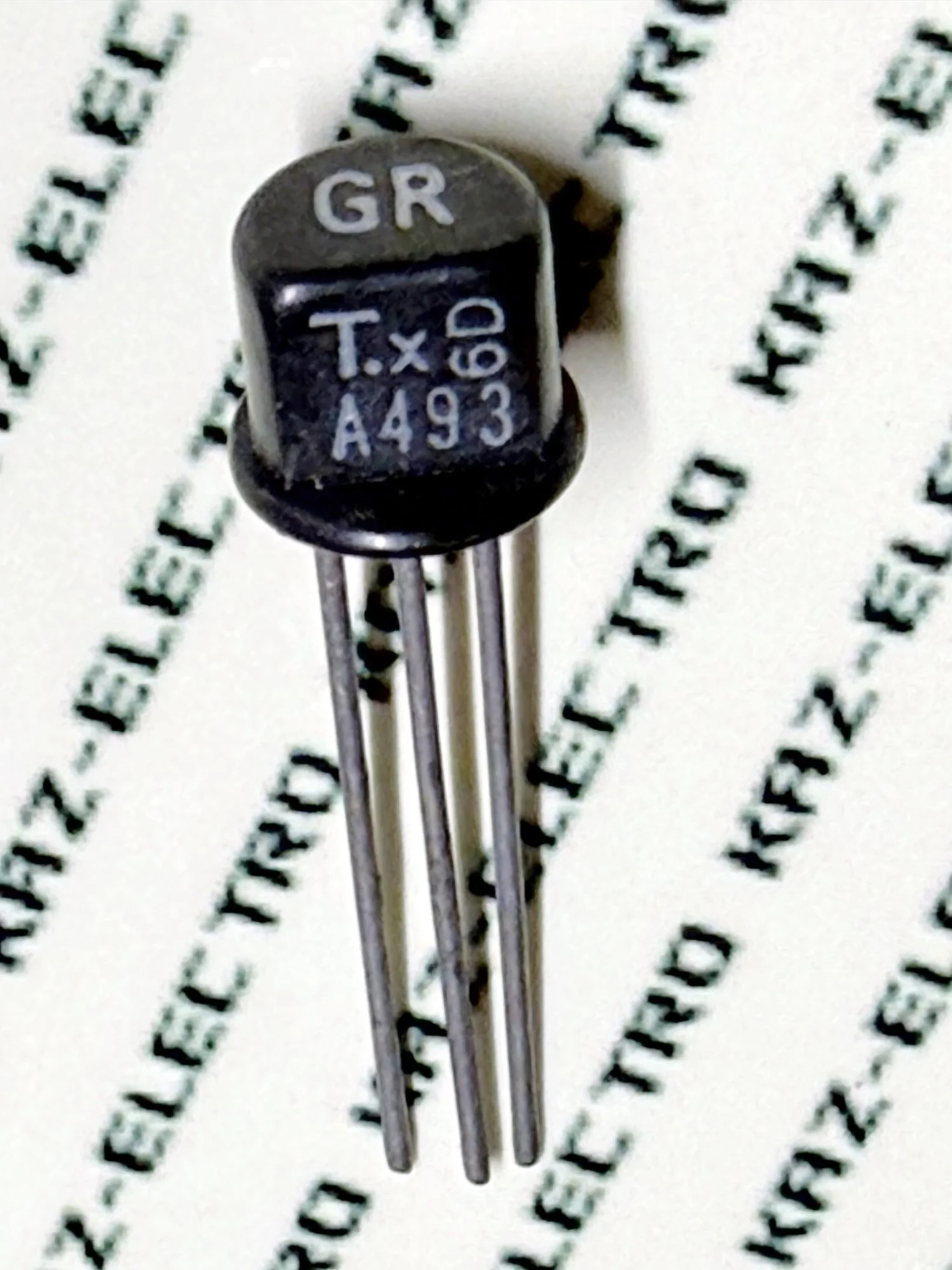
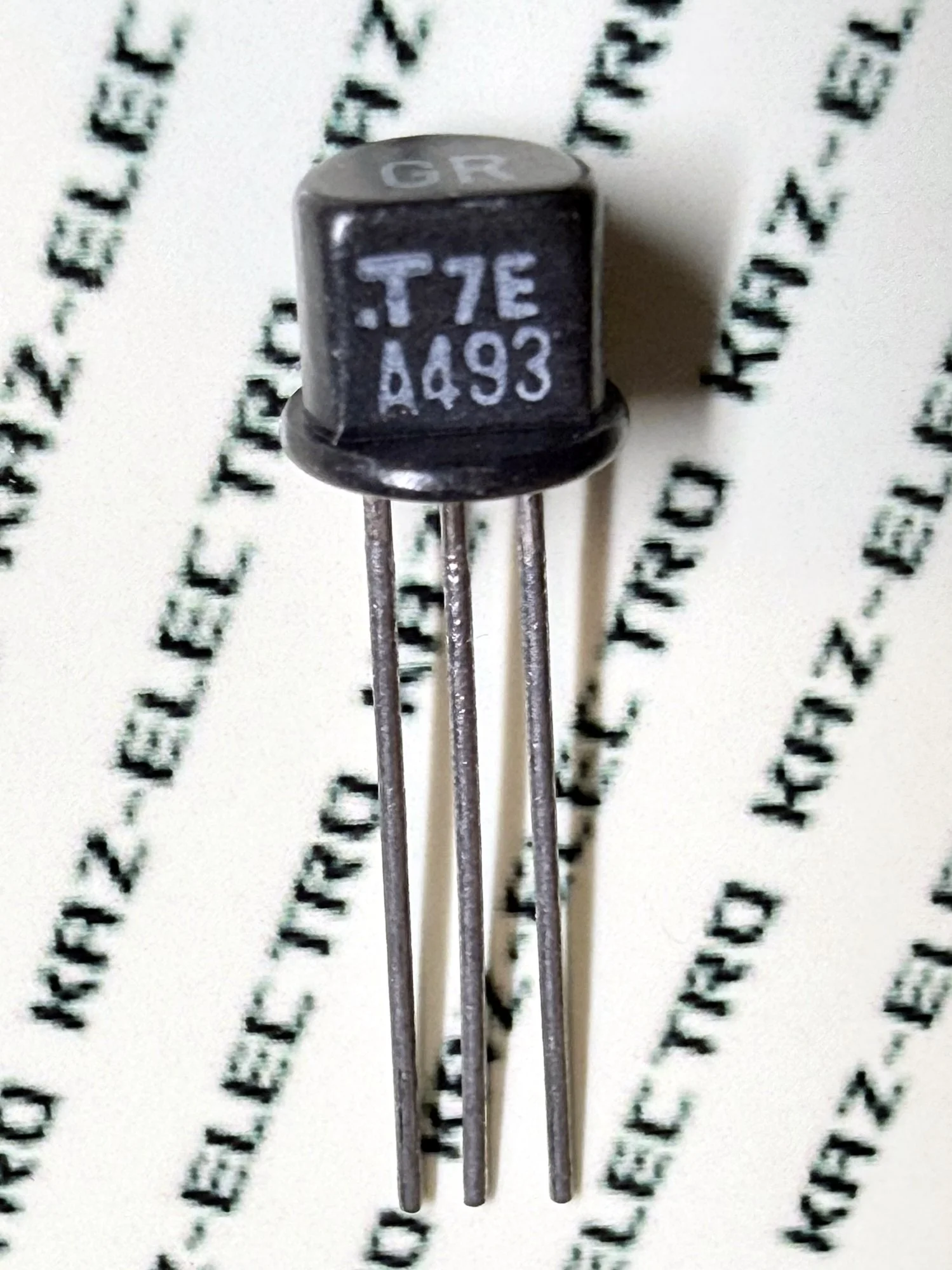
Toshiba transistors bearing an “X” mark are frequently encountered. The meaning remains unresolved, but the mark is most common on units from the relatively later production period, from around 1973 onward.
This is not confined to the 2SA493/2SC1000 family. “X”-marked units have been confirmed across a wide range of 1970s–80s long-running products, both consumer-grade and Telecom/Industrial: the 2SA503/2SC503 (TO-39; → No.50), the 2SA509G/2SC509G (Toshiba proprietary package, Green Series), the 2SA505/2SC495 (TO-126), and the 2SA473/2SC1173 (TO-220), among others.
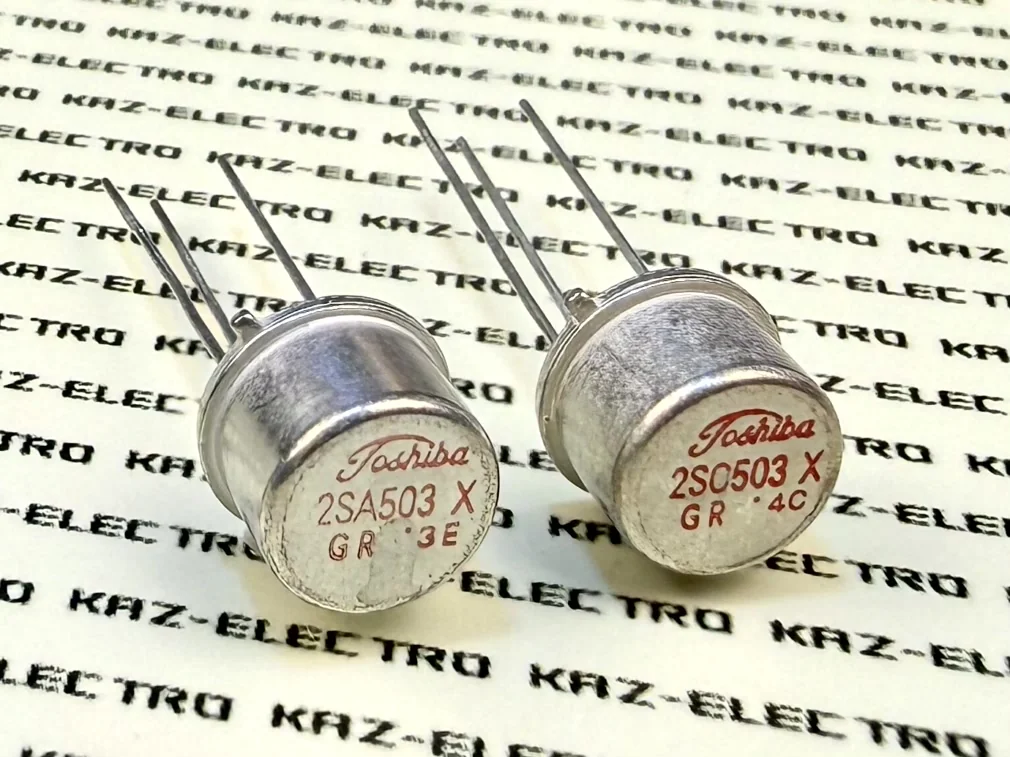
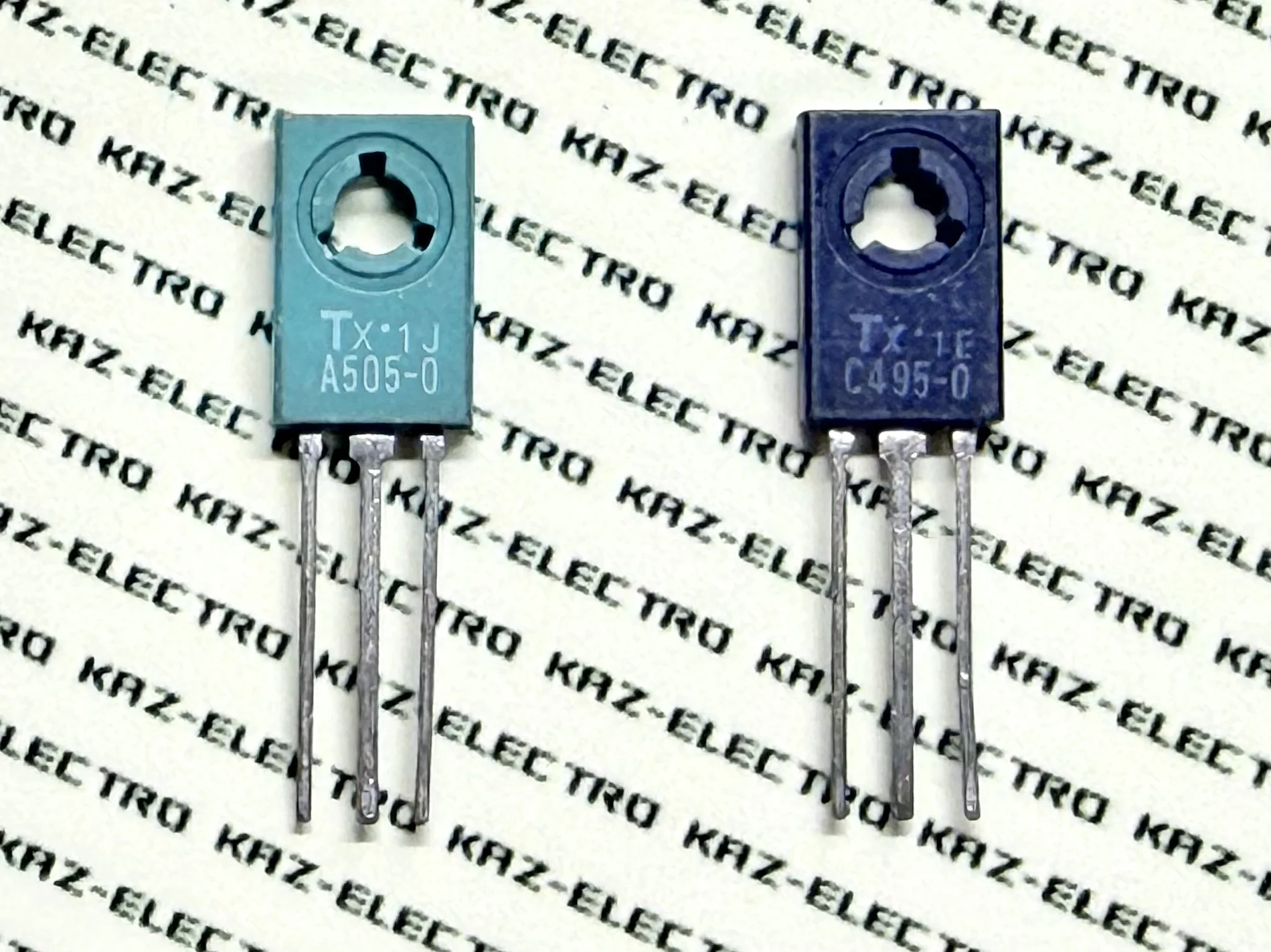
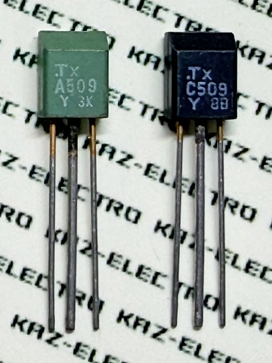
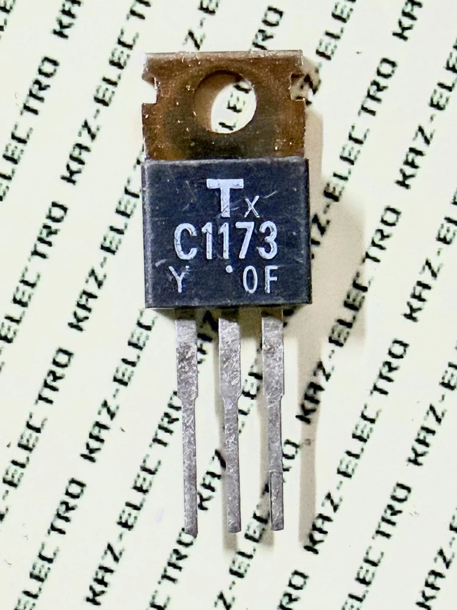
Packaging boxes with “2SC594X-Y” and similar designations explicitly printed on the part number field have also been observed, suggesting deliberate intent behind the suffix.
In the author’s earlier reasoning, the absence of “X” marks on older units bearing katakana lot markings suggested a possible link to NRND (“maintenance-designated”) status. But as the photographs above show, even among final-generation TO-98 units of the same part number, X-marked and non-X-marked examples from 1977–1979 coexist — and the origin remains unresolved.
The author’s current working hypothesis is that the “X” mark may have been applied to lots or lines where some manufacturing process or method had been updated, to allow internal distinction from earlier-process units. However, since X marks became nearly universal in later years, this explanation has its limitations.
There is also an interesting temporal pattern. “X” marks, which appeared broadly from the early 1970s onward, effectively disappear from resin-package products by the early 1980s. On metal-can (CAN) package products such as TO-39, scattered X marks continue to appear beyond that point. This may relate to the fact that resin-package products underwent a manufacturing process overhaul — the “rationalization” described in this chapter — while CAN-package lines continued on older equipment. Whether that connection holds is a question the author cannot yet answer.
If any reader has information on the meaning of the “X” mark, the author would very much welcome contact. A fuller treatment of the origin and disappearance of the X mark lies beyond the scope of this article and is reserved for a separate piece.
10.5 The Transition in Packaging Technology
The TO-98 Manufacturing Process (Estimated)
The production process is estimated to have resembled that used for CAN-package devices such as the TO-18 and TO-72:
- Prepare the top-hat-shaped epoxy resin package body
- Set the package body upside-down in a holding jig
- Insert the round-pin lead assembly with silicon die already mounted and wire-bonded
- Inject liquid epoxy resin to fill the package body
- Cure under heat to complete
The characteristic “brim” of the silk-hat shape likely served to prevent the package body from falling through the holding jig during assembly — this is the author’s inference rather than confirmed fact.
In the author’s reading, the actual production flow involved loading package bodies upside-down into jigs, then moving the jigs sequentially from the resin injection station to the curing oven — a step-and-cure assembly method.
The TO-92 Manufacturing Process
The TO-92 transistor, still produced worldwide today, uses transfer molding — a cavity-based integral forming method in which resin is injected under high pressure into a mold and formed in a short cycle. Lead-frame “hoop” (continuous strip) production became possible, and manufacturing throughput increased dramatically.
The disappearance of TO-98 products around 1980 is best understood against this backdrop of manufacturing technology advancement. The pursuit of cost reduction and capacity expansion through continuous production was what drove Toshiba and Japan’s other semiconductor manufacturers toward transfer molding.
TO-98 vs. TO-92: External Comparison
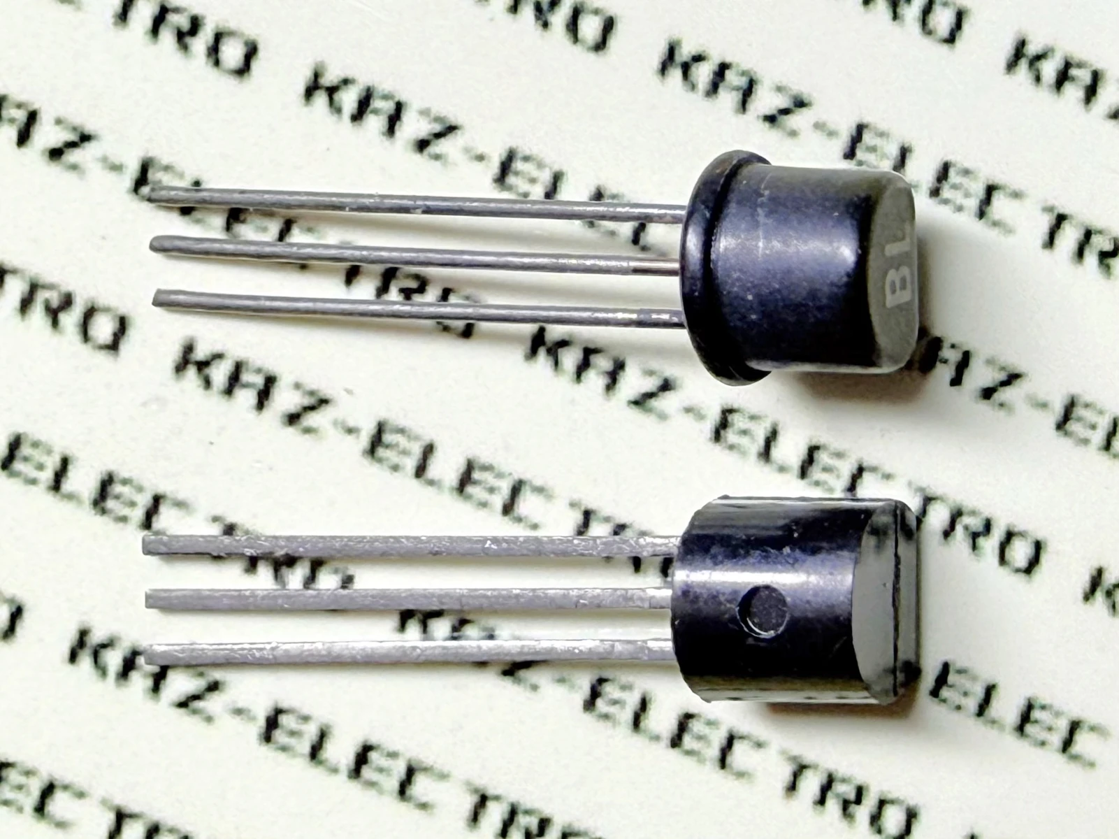
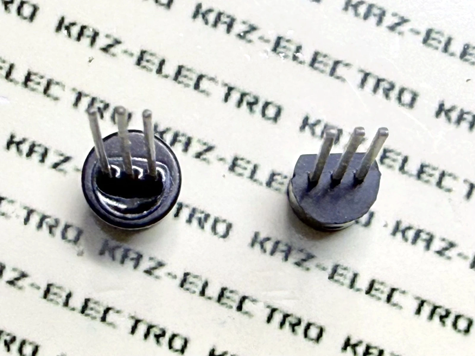
One detail not visible in the photographs: TO-98 leads are round-pin type, made from iron-based material with solder plating, while TO-92 uses a lead-frame construction in copper-based material with solder plating.
The change to copper lead frames also improved thermal conductivity. Notably, the TM conversion wave extended beyond TO-98 products. Toshiba’s proprietary 2-5S package — used for mini-power transistors in the ~0.6W Pc class, such as the 2SA661/2SC1166 and 2SA509/2SC509 — was also converted to TO-92 during the same period. The shift from iron-based round-pin leads to copper-based lead frames is a plausible contributor to the improvement in collector dissipation Pc seen in the GTM series.
Transfer Molding Transitions Across Manufacturers
The shift to transfer molding was not confined to Toshiba; it extended across Japan’s semiconductor industry. However, each manufacturer handled the part-number implications of the packaging change differently.
| Manufacturer | Previous (old package) | New package | Part number change | Approximate timing |
|---|---|---|---|---|
| Toshiba | TO-98 (potting type) | TO-92 | Yes (TM suffix) | c. 1978 |
| NEC | TO-92 (potting type) | TO-92 | No | Early 1970s |
| Hitachi | Rectangular (potting type) | Rectangular (transfer mold) | No | Mid-1970s |
| Rectangular (transfer mold) | TO-92 | No | c. 1978 | |
| Matsushita | TO-92 (potting type) | TO-92 | No | Late 1970s |
| Sanyo | Hemisphere (potting type) | TO-92S / TO-92 | SP/NP | Mid-1970s |
| TO-92-like (potting type) | TO-92 (transfer mold) | No | Mid-1970s |
For some products from Toshiba, Matsushita, and Sanyo, maximum ratings such as Pc (collector dissipation) changed with the transfer molding transition.
Matsushita is the present-day Panasonic. The brand name in use at the time was “National.”
Mitsubishi and Sony are currently under investigation; the author has not yet personally encountered potting-type examples from either manufacturer.
NEC
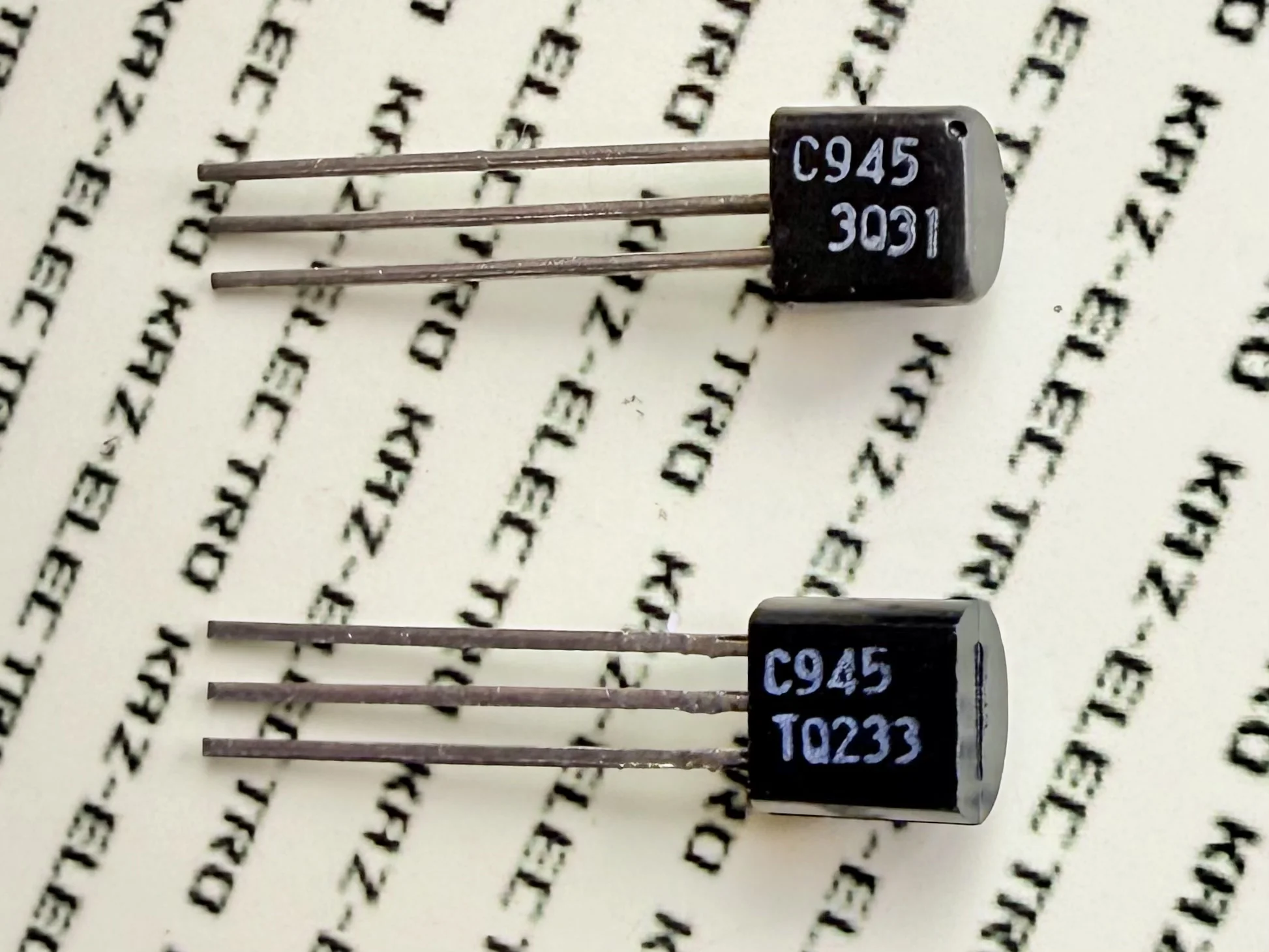
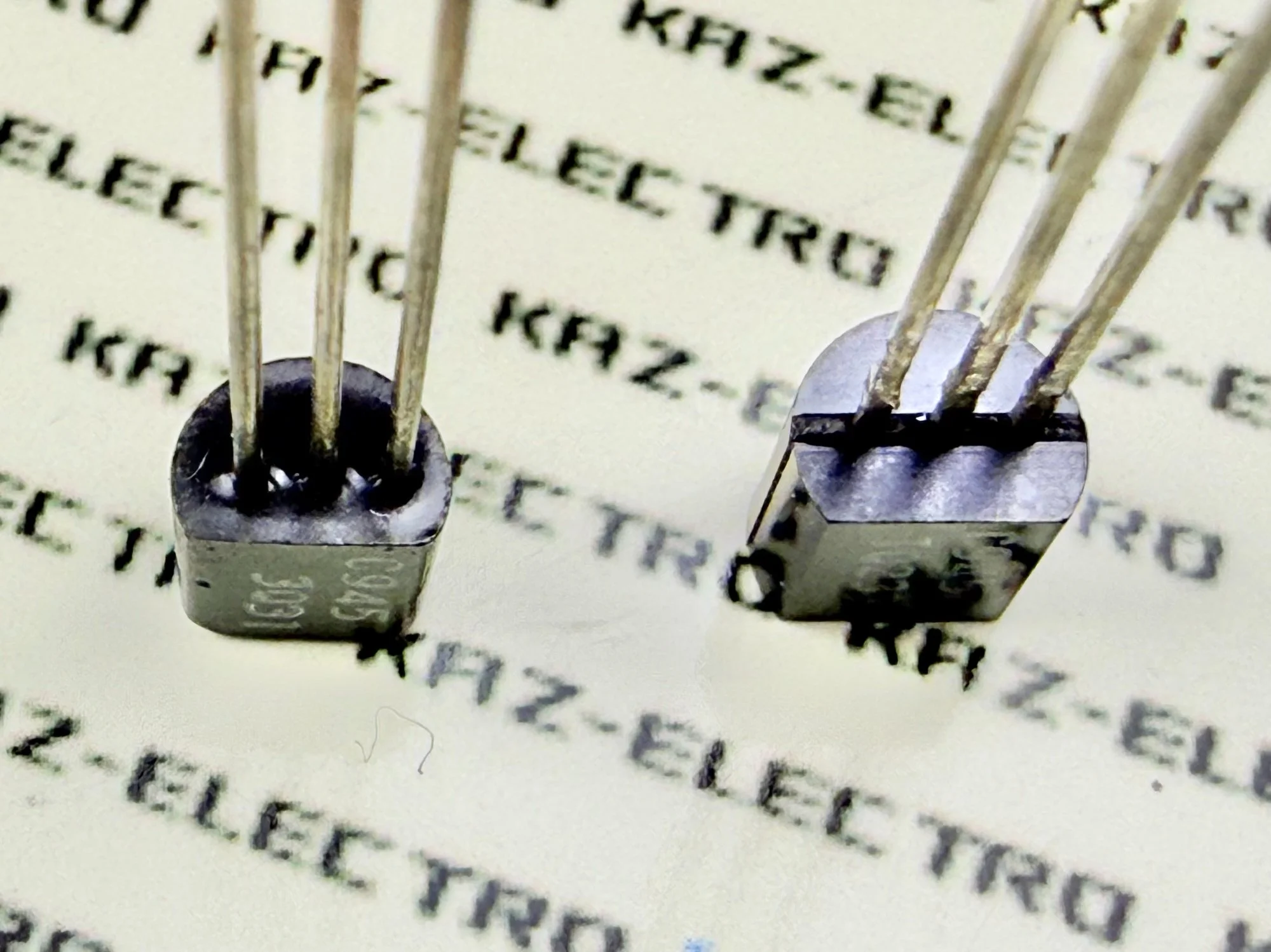
Hitachi
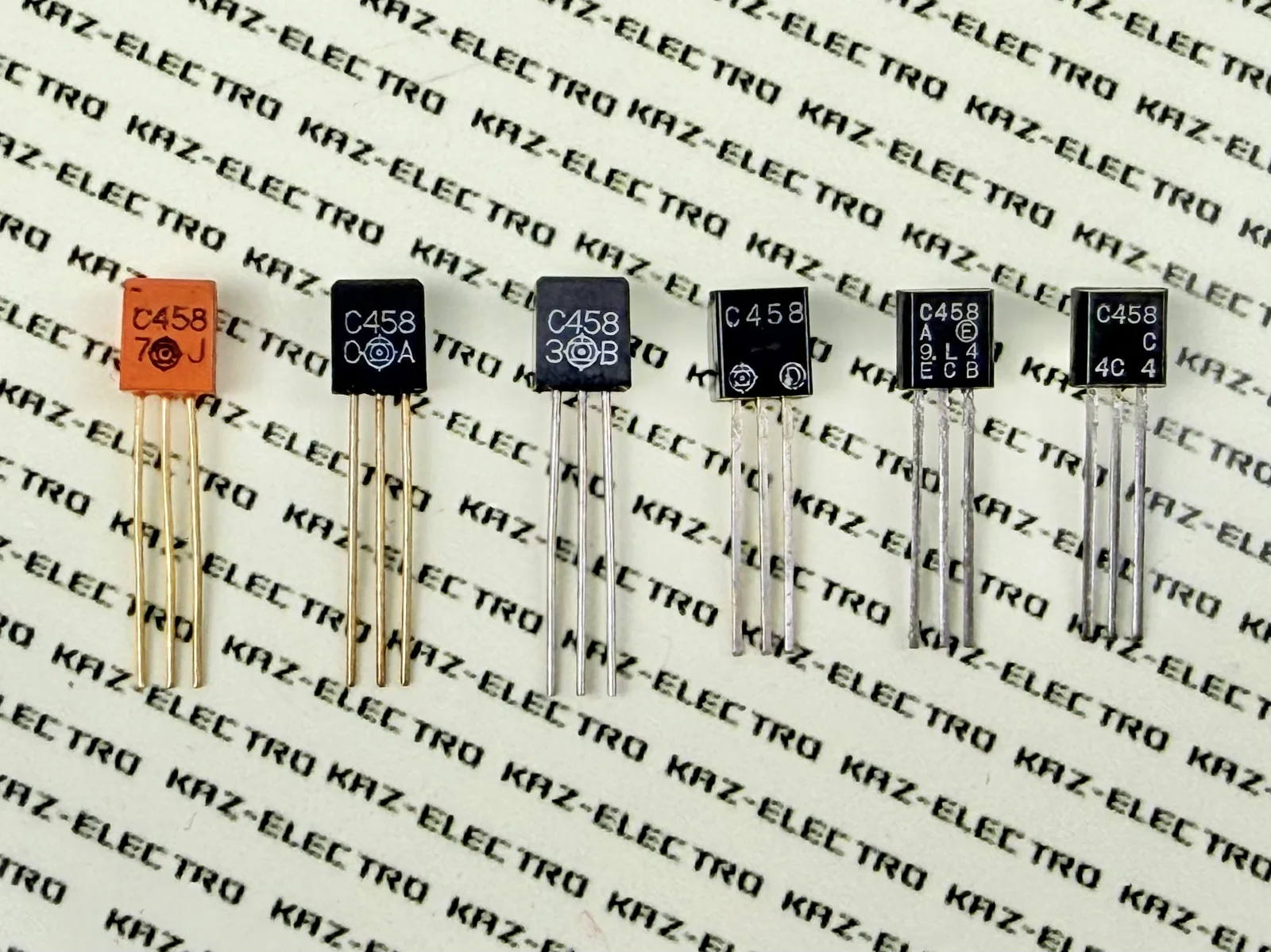
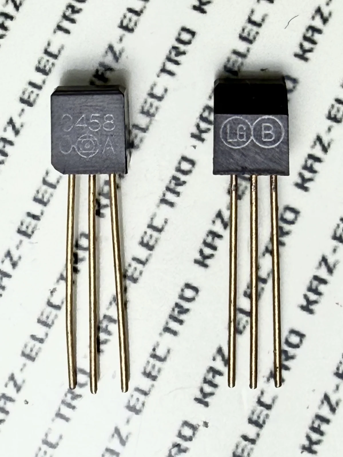
Matsushita
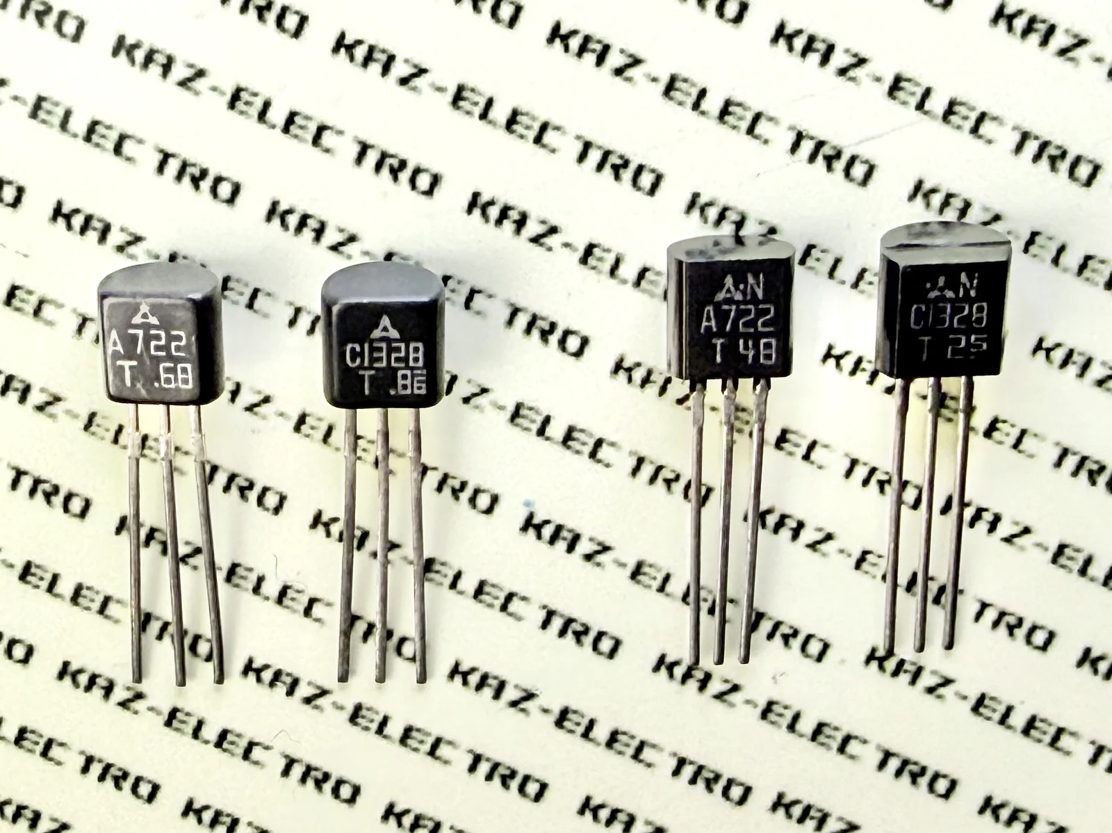
Sanyo
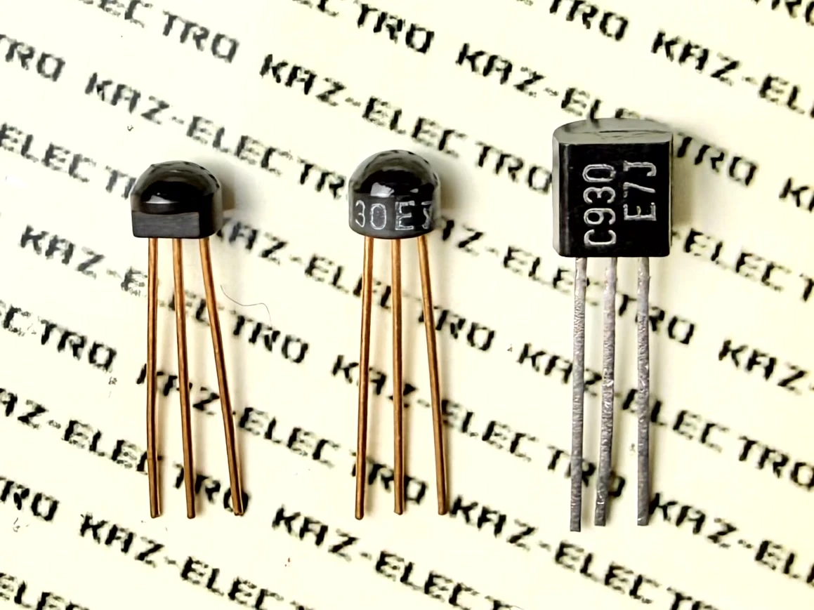
Because other manufacturers made the packaging transition without changing the part number, examples of the same part number produced in different eras may have different package types. The author plans to address each of these on a product-by-product basis in future articles.
10.5.1 The Birth of the GTM Family
As discussed in Chapter 5, the transition to TM packaging extended to the 2SA493G/2SC1000G, giving rise to the 2SA493GTM/2SC1000GTM.
The products listed below were introduced as Green Series TO-98 devices in the same manner as the 2SA493G/2SC1000G during the 1960s and 1970s, and continued in production for extended periods after their conversion to TO-92 from 1980 onward. These form the GTM family; full datasheets were available for all of them.
| Part Number | Application |
|---|---|
| 2SA429GTM / 2SC780AGTM | High-voltage switching |
| 2SA467GTM / 2SC366GTM, 2SC367GTM | RF medium-power amplification / medium-power pulse amplification |
| 2SA493GTM / 2SC1000GTM | Low-frequency, low-noise amplification |
| 2SA509GTM / 2SC509GTM | Audio power amplification / switching |
| 2SC752GTM | Ultra-high-speed switching |
| 2SC387AGTM | UHF amplification |
| 2SC980AGTM | RF amplification / high-speed switching |
Industrial and professional equipment tends to use classical discrete circuit designs. Unlike consumer products, which follow fashion cycles, industrial equipment prioritizes long service life and proven operating history — once a device is designed in, it tends to stay in use for years or decades. The persistent transistor demand in switching applications reflected this. The GTM family served that demand; within it, the 2SA493GTM/2SC1000GTM stood apart as the only device in the Green Series explicitly positioned for low-noise use.
10.5.2 The Birth of the TM Family
The transition to TM packaging was not limited to the Green Series; it extended to standard consumer-grade products as well (see Chapter 6).
While the range was not large, some products survived the wave of TO-98 discontinuations that swept through 1980, carrying forward into TO-92 form. These devices had full characteristic curves in their datasheets, and production and sales continued into the 2000s.
Surviving TM Products
| Part Number | Application |
|---|---|
| 2SC380TM | FM radio IF amplification |
| 2SC382TM, 2SC383TM | Television IF amplification |
| 2SC732TM | Audio low-noise amplification |
| 2SC941TM | AM radio RF amplification |
| 2SC982TM | Darlington |
| 2SK19TM | VHF general-purpose JFET |
| 2SK30ATM | Audio low-noise amplification JFET |
The 2SK19TM alone was replaced by the successor 2SK192A and discontinued in the early 1980s.
Products that were technically mature by 1980 and required no significant revision — particularly those with sustained demand — survived the TO-92 transition and remained in production into the 2000s.
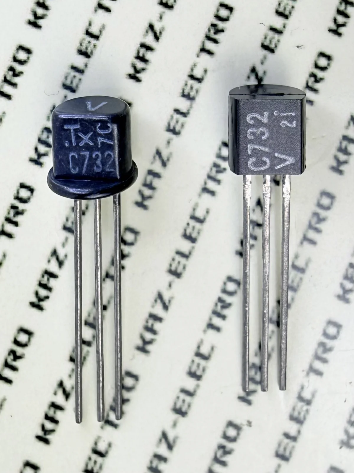
The V rank is a special-selected grade not listed in standard catalogues, handled separately from the standard ranks (GR, BL). Details of the V rank are addressed in a separate section. The 2SC732TM itself, like the 2SA1015/2SC1815, was a long-running product that remained in production until the major Toshiba discrete device consolidation of 2012.
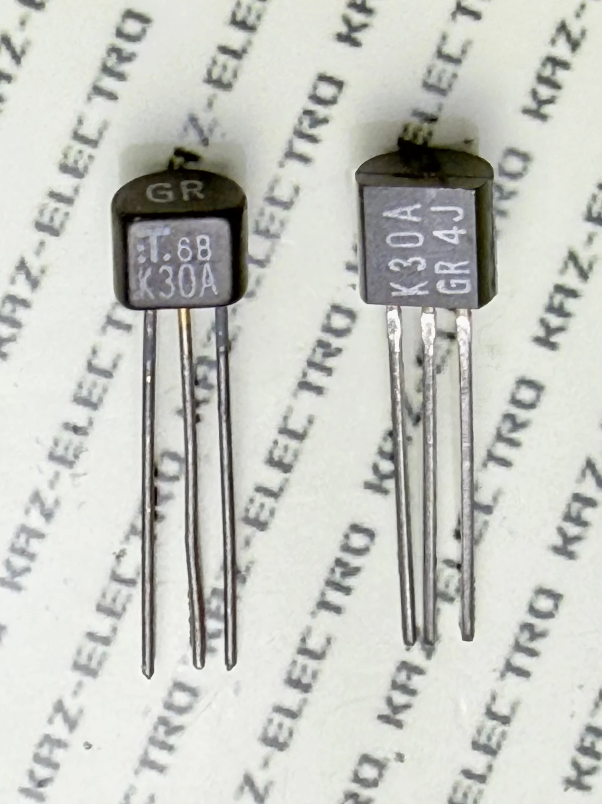
The 2SK30A-GR (1976) at left uses Toshiba’s proprietary 2-5U package — a TO-98 (Toshiba internal designation: 2-5J) with the flange removed. The author’s current hypothesis is that this form factor was intended for differential amplifier input stages where two devices are mounted in close contact for thermal coupling, but details will be addressed in a dedicated article. The predecessor 2SK30 first appeared in the 1971 databook. Like the 2SC732TM, it became a long-running product spanning approximately forty years.
The existence of unlisted-datasheet TM devices such as the 2SC1000TM, and the context surrounding them, is discussed in detail in Chapter 6.
10.5.3 The TM Suffix: Meaning and Rating Changes
By explicitly adding the “TM” suffix, Toshiba signaled that a packaging transition had occurred while the core part identity was maintained. A part number change — even to an upward-compatible successor — would have triggered re-qualification requirements under standard component approval practices. In that light, this naming approach was not simply a cataloguing convenience; it was, in the author’s reading, a gesture of consideration toward users.
More specifically, the EIAJ convention calls for suffixes such as A, B, C… to indicate improved versions (e.g., 2SC1000A). Toshiba deliberately set this aside and instead used “TM,” signaling to the market that the change was one of package form only, not a functional revision.
This interpretation is based on long-term observation of actual units and contemporary databooks. It does not derive from any internal Toshiba documentation.
Rating changes associated with TM conversion varied substantially by product — from effectively no change in some cases, to significant improvements in voltage rating, Pc, and Ic in others.
Rating Changes with TM Conversion — Variation by Product
| Product | Major rating changes | Nature of change |
|---|---|---|
| 2SK30ATM | No change | Package form only |
| 2SC387AGTM | Pc: 0.2 → 0.25 W | Minor improvement |
| 2SC380TM | Ic: 30 → 50 mA, Pc: 0.2 → 0.3 W | Moderate improvement |
| 2SC383TM | Vcbo: 75 → 50 V, Vceo: 40 → 45 V, Vebo: 3 → 4 V | Voltage rebalancing (partial reduction) |
| 2SA493GTM / 2SC1000GTM | Substantial improvement in voltage, Pc, and Ic | Major improvement |
| 2SA495GTM / 2SC372GTM | Substantial improvement in voltage, Pc, and Ic | Major improvement |
| 2SC732TM | Substantial improvement in voltage, Pc, and Ic | Major improvement |
The substantial rating improvements in the 2SA493GTM/2SC1000GTM, 2SA495GTM/2SC372GTM, and 2SC732TM are notable, and their ratings and characteristic curves bear close resemblance to those of the 2SA1015/2SC1815. A trend analysis based on measured data is presented in Section 11.8. Detailed SPICE parameters and quantitative comparisons are reserved for a separate article.
10.5.4 Unofficial TM Survivors
Section 6.3 noted that most unlisted-datasheet TM variants remained in production for only a brief window — roughly 1980 to 1983. Some, however, proved surprisingly persistent.
The 2SA495/2SC372 is a 30V-rated general-purpose small-signal complementary pair — from the days when radio enthusiasts and professional engineers alike kept it as a standard part. This family also has its unofficial TM variants, and lots of the 2SC372TM from 1984 are not uncommon in the author’s collection. While most of its counterparts had disappeared by 1983, the 2SC372TM lingered roughly a year longer.
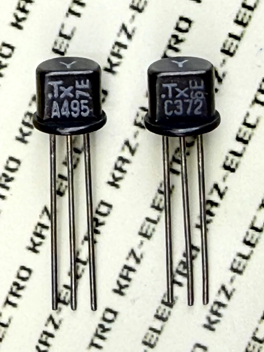
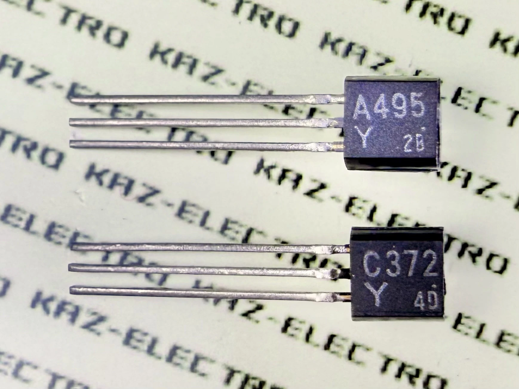
These unofficial TM variants were produced in parallel with the official successor — the 2SA495GTM/2SC372GTM listed in Section 10.5.1’s GTM table — which had full databook coverage of its ratings and specifications. The unofficial TM version was running alongside an officially documented successor, unannounced and unlisted.
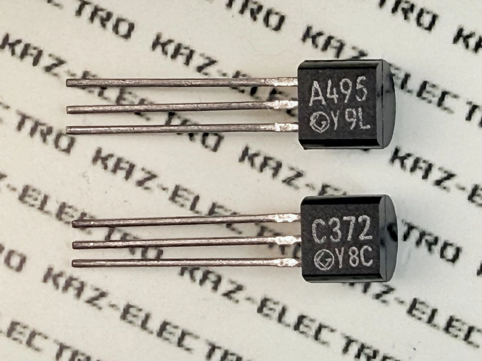
The 2SA509TM/2SC509TM presents an even more puzzling case.
The predecessor 2SA509/2SC509 was a resin-molded mini-power transistor introduced in Toshiba’s proprietary rectangular “TOSHIBA 2-5S” package (the same form factor as the 2SA661/2SC1166 discussed in Section 6.3) — another standard device of the era, as familiar as the 2SA495/2SC372. By the late 1970s, the rationalization wave reached this family too; the standard-grade 2SA509/2SC509 received NRND designation, while the high-reliability grade 2SA509G/2SC509G was converted to TO-92 and continued as the 2SA509GTM/2SC509GTM.
With this, the other TO-98 product families also became subject to reorganization. The consumer-grade mainstream passed to the next generation as the rationalization wave moved through.
Yet the original 2SA509/2SC509, which should have been NRND since 1979, appears to have quietly undergone its own TM conversion — just as the 2SC1000 did — and continued in production as late as 1986. (The author was entirely unaware of this until recently.)
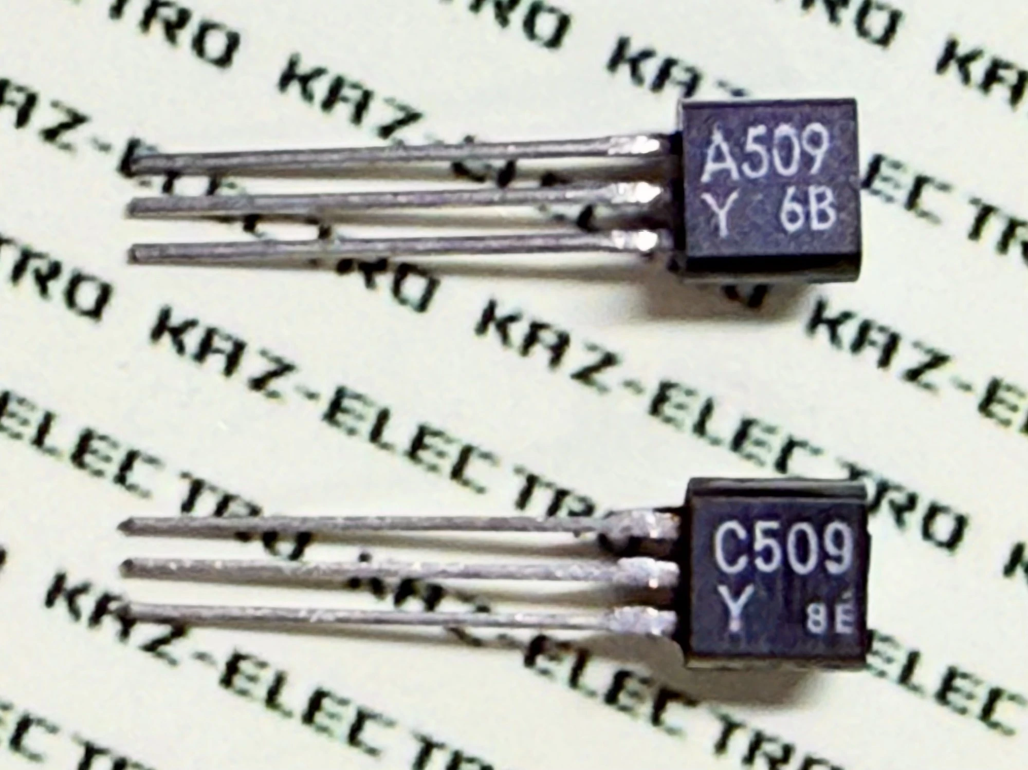
And here is the official GTM successor:
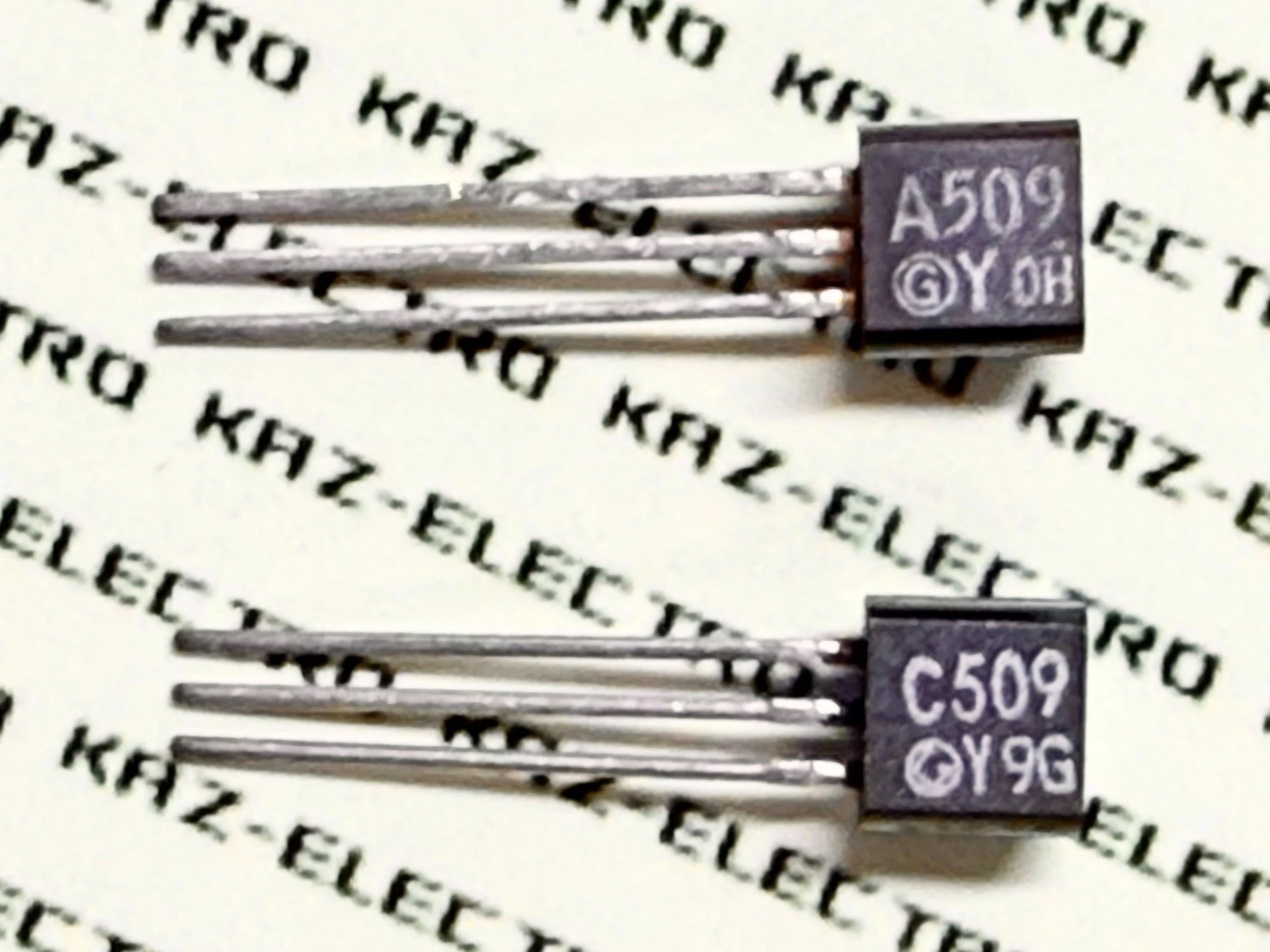
Why unofficial TM variants continued to be produced in parallel with official successors — the author has no definitive answer at this time. The G-grade high-reliability products were converted to TM and continued in production to ensure long-term stable supply for industrial applications. It is possible that, for the standard consumer-grade versions — given their status as established staples — residual demand persisted quietly, and low-volume production continued to serve it. The picture that emerges is of both official and unofficial products responding flexibly to individual demand, regardless of what the databooks stated. This phenomenon of “official and unofficial running in parallel” connects directly to the world of the 2SA493GTM/2SC1000GTM at the center of this article, and the author hopes to address it in a dedicated piece in due course.
[Chapter 10 Summary] The transformation traced in this chapter — from 1978 through 1981 — is the history of the transistor completing its evolution from a crafted object into an industrial product.
The hand-applied color dots, the unhurried top-face markings, the two-face printing bearing the “T” logo — the functional elegance of the TO-98 era was stripped away by the demands of high-speed automated production.
But this was not simply “simplification.” It was a rational outcome driven from the factory floor — the means by which Japan’s semiconductor industry built and sustained its competitiveness in world markets. The changes in the external appearance of the transistors that passed through engineers’ hands are, precisely, the record of that age of the torrent.
11. Verification: Characteristics Comparisons and Measured Data
The 2SA493/2SC1000 family has been examined from many angles throughout this article, and its year-by-year specification changes have proved complex and difficult to untangle. This chapter opens with a focused look at the differences between family members — specifically, what the hFE–Ic curve shapes in the datebooks reveal — in an attempt to clarify what changed and when. As noted in Section 10.5.3, the GTM type saw substantial rating increases; this goes beyond a packaging change, and the possibility that the die itself was revised cannot be ruled out. The second half of the chapter turns to measured data, gathered using the author’s custom instruments, to put these questions to the test.
Questions examined in this chapter
- How closely does the replacement pair 2SA970/2SC2240 match the original 2SA493/2SC1000? (Section 11.1)
- Is there a measurable difference in characteristics between the unmarked original type and the G type? (Section 11.2)
- What, specifically, changed between the G type and the GTM type? (Section 11.3)
- Measured verification of the GTM type — tracing the possibility of a die change through actual data (Sections 11.4–11.10)
11.1 Original Type vs. Replacement (2SA970/2SC2240)
Among the replacement options for the 2SA493/2SC1000 complementary pair, the most accessible is the 2SA970/2SC2240.
The 2SA970/2SC2240 emerged around 1980 as Toshiba’s designated successor and remained in production for over 30 years — the mainstream of Toshiba’s low-noise line until the very end of the discrete device era. As of 2025, NOS (New Old Stock) units can still be found at Japanese electronics retailers and on eBay.
The question of how these long-lived successors compare to their predecessor is a natural one. The author compared the hFE–Ic characteristics of both pairs using datebook data.
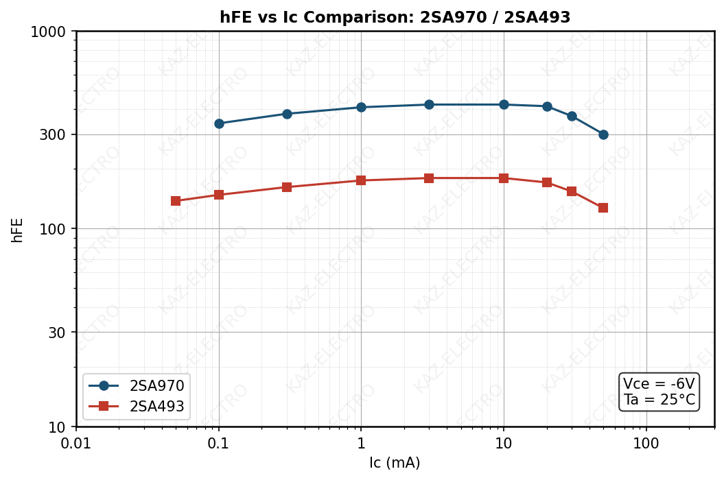
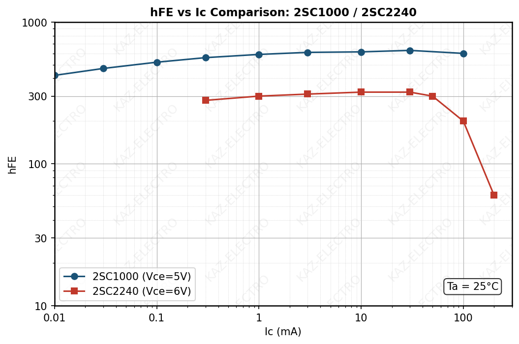
PNP side (2SA493 vs. 2SA970)
The peak hFE of the 2SA970 is approximately 370 — nearly twice that of the 2SA493 (approximately 180). Direct substitution may therefore require bias adjustment. Both devices, however, share a gently rounded curve shape with a peak in the 3–10 mA range, and the overall character is similar.
NPN side (2SC1000 vs. 2SC2240)
The 2SC1000 peaks at approximately 440; the 2SC2240 at approximately 320 — a difference of roughly 1.4×. A detailed shape comparison follows in the next section using normalized curves.
11.1.1 Curve Shape Comparison (Normalized)
Toshiba datebook hFE–Ic graphs show only a “representative (average)” value without specifying the hFE rank (Y/GR/BL, etc.). This makes it impossible to determine whether differences in absolute values reflect the rank of the particular sample plotted, or the true population average of the device type.
To address this, the author prepared normalized graphs — scaling each curve so that its peak value equals 1.0 — enabling a comparison of curve shape independent of absolute hFE.
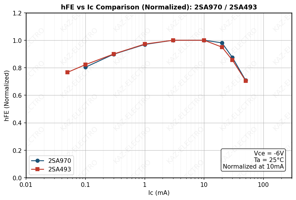
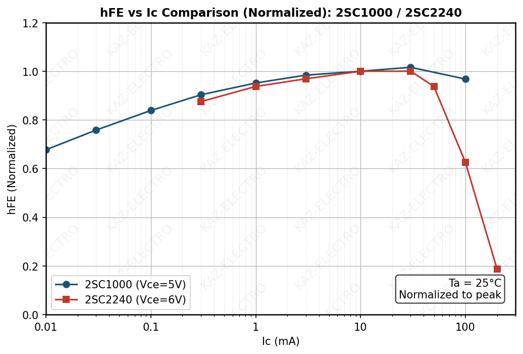
PNP side (2SA493 vs. 2SA970)
The curve shapes are nearly identical. Both peak in the 3–10 mA range, and the rate of decline at low and high current follows the same pattern. A clear continuity of design intent is readable from these curves.
NPN side (2SC1000 vs. 2SC2240)
Low-noise transistors are used primarily in applications such as the input stage of equalizer amplifiers, where operating currents typically fall in the 0.1 mA to several mA range. Within this practical window, the hFE–Ic curves of both devices overlap closely, showing high interchangeability. Above 100 mA the behavior diverges, but small-signal transistors are rarely operated in that region, so this difference has no practical consequence. The 2SC2240 can be used as a drop-in replacement without issue.
[Supplementary note] hFE notation styles by manufacturer
Manufacturers differ in how they present hFE–Ic curves. The following summary may be useful when reading datasheets from different sources.
- Toshiba: representative (average) value only; hFE rank not shown
- Mitsubishi: normalized graph (peak = 1.0), showing shape only
- Sanken: both Min and Max plotted
Sources: TOSHIBA Semiconductor Handbook 1975 / Databook 1980
『最新トランジスタ互換表』 (CQ Publishing, 1970–1982); 『最新トランジスタ規格表』 (CQ Publishing, 1968–1988)
11.2 Original Type vs. G Type
The hFE–Ic characteristics of the original 2SA493/2SC1000 and the Green Series 2SA493G/2SC1000G are compared below, using curves from the published datasheets.
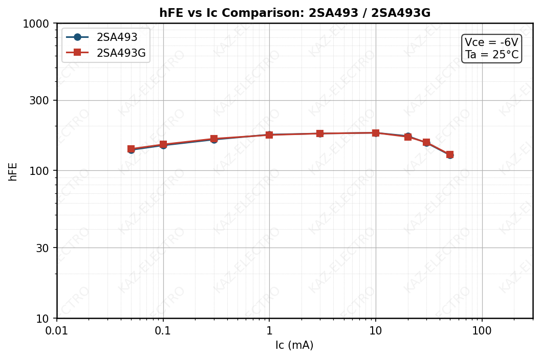
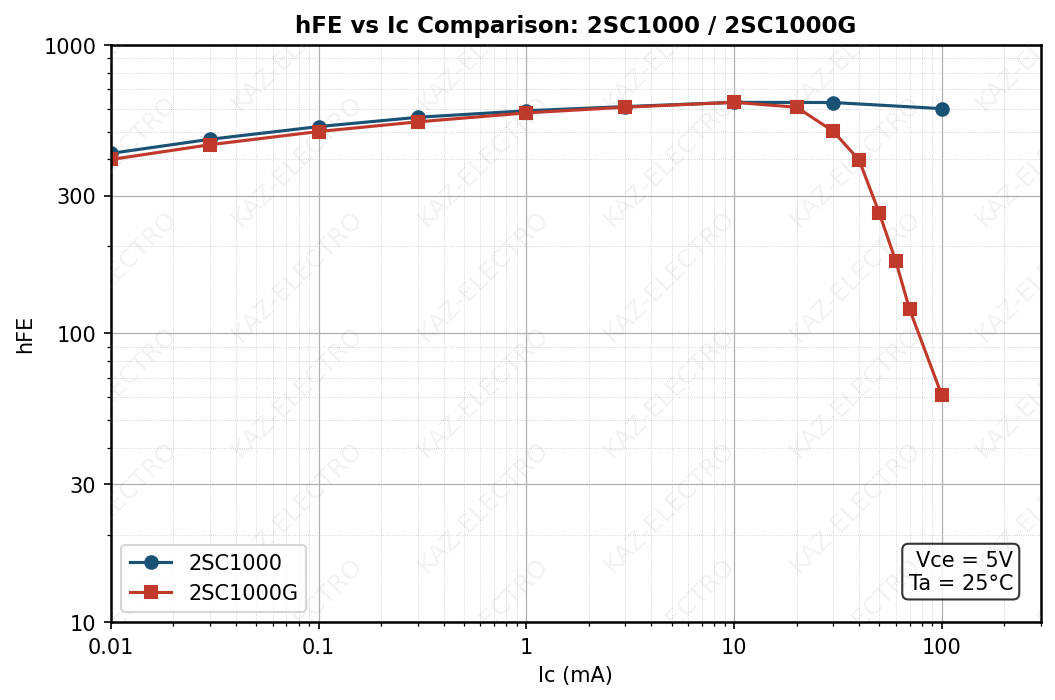
PNP side (2SA493 vs. 2SA493G)
Both devices peak at approximately hFE = 180, and the curves are nearly coincident. The characteristic decline to approximately 125 at 50 mA, following a broad peak around 10 mA, is shared by both.
NPN side (2SC1000 vs. 2SC1000G)
At low currents (up to ~10 mA), both devices peak at hFE ≈ 630. Above that, the curves diverge. The standard 2SC1000 maintains hFE ≈ 400 even at 100 mA, while the 2SC1000G drops sharply beyond 20 mA, falling to approximately 60 at 100 mA.
Sources: TOSHIBA Semiconductor Handbook 1973/1975, Databook 1977
11.2.1 Curve Shape Comparison (Normalized)
Normalized graphs (peak = 1.0) are used to isolate and compare curve shape.
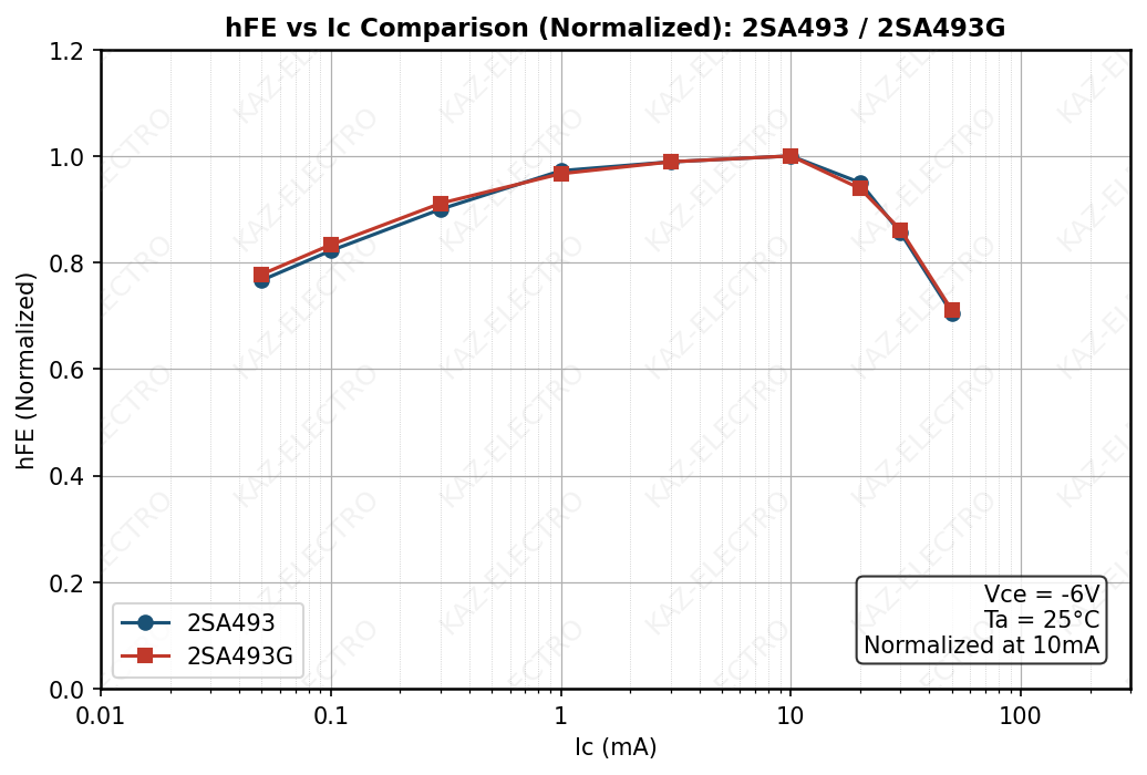
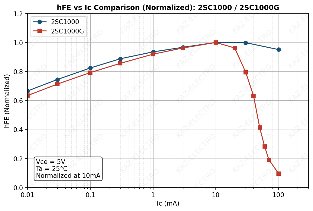
PNP side (2SA493 vs. 2SA493G)
When normalized, the two curves are nearly indistinguishable. This supports the interpretation that both devices were selected from dies fabricated through the same process. Toshiba’s own documentation states that the G type underwent more rigorous testing, inspection, and burn-in than the original type.
NPN side (2SC1000 vs. 2SC1000G)
At low currents (up to ~10 mA), the shapes are nearly identical. At higher currents, the behavior diverges markedly. The 2SC1000 holds a normalized value of 0.95 at 100 mA — essentially flat — while the 2SC1000G drops precipitously above 20 mA, falling to 0.1 at 100 mA.
On the NPN divergence
The reason for this difference is not clear. The author checked Toshiba datebooks from 1973 through 1977 and found the same curves reproduced consistently across editions. A printing error in measurement conditions cannot be entirely ruled out, but this archive reproduces the datebook data as recorded.
Sources: TOSHIBA Semiconductor Handbook 1975, Databook 1977
11.3 G Type vs. GTM Type
The hFE–Ic datebook curves for the Telecom/Industrial Green Series are compared across the original G type (TO-98) and the GTM type (TO-92).
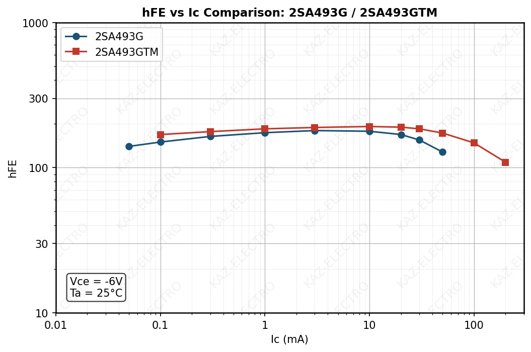
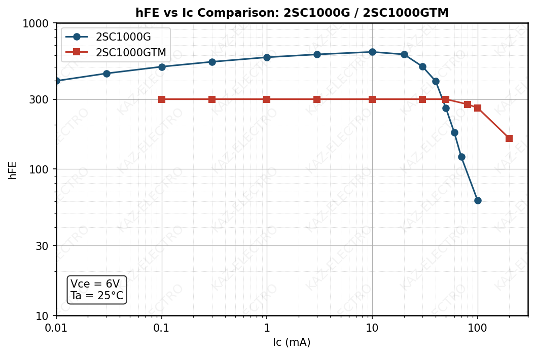
PNP side (2SA493G vs. 2SA493GTM)
The 2SA493G peaks at hFE ≈ 180 in the 3–10 mA range. The 2SA493GTM peaks at hFE ≈ 192 — essentially the same — and maintains compatibility. At high currents, characteristics show improvement.
NPN side (2SC1000G vs. 2SC1000GTM)
The 2SC1000G peaks at hFE ≈ 630, but drops sharply at high currents, falling to approximately 60 at 100 mA. The 2SC1000GTM, by contrast, holds hFE ≈ 300 across the entire 0.1–50 mA range in a remarkably flat characteristic, and remains at approximately 260 even at 100 mA. The GTM is far more stable across a wider current range.
11.3.1 Curve Shape Comparison (Normalized)
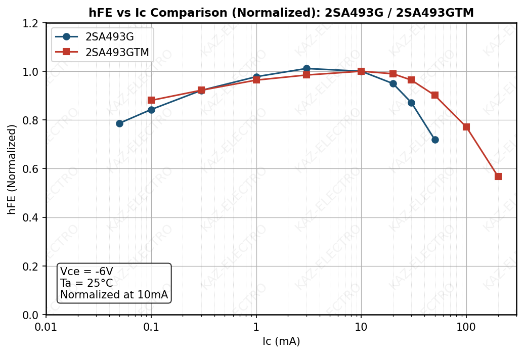
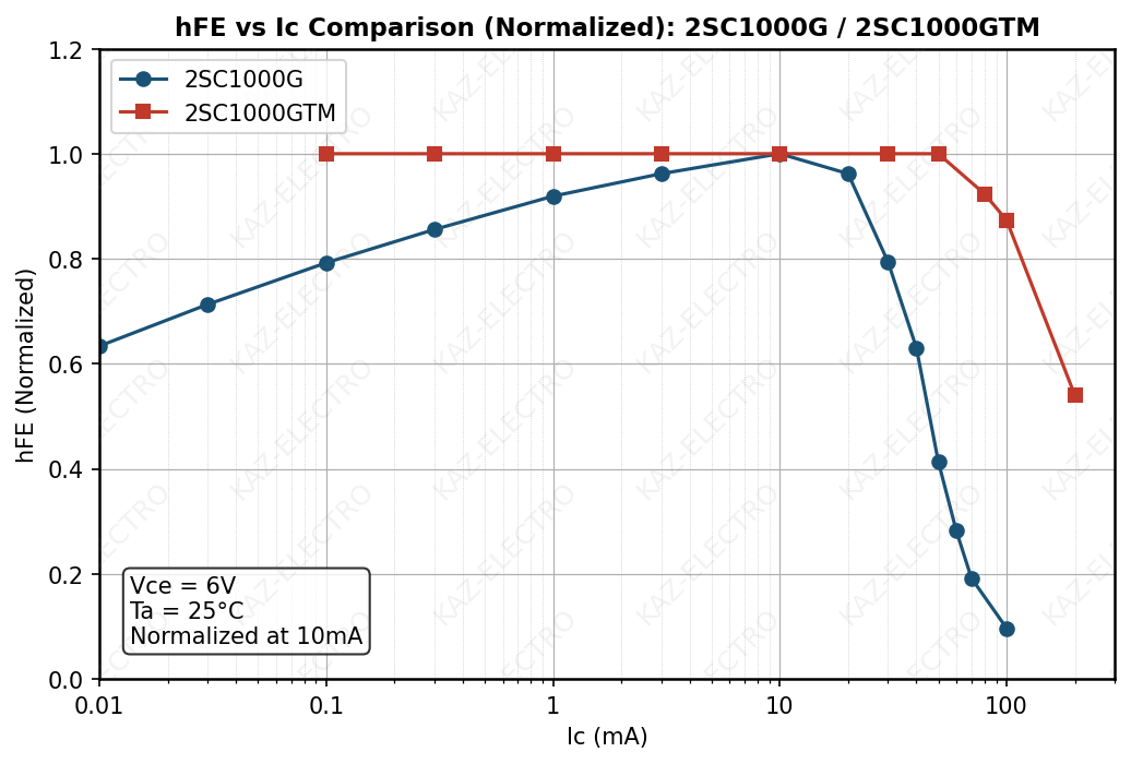
PNP side
Curve shapes are similar, though the GTM shows a gentler roll-off at high currents.
NPN side
The shapes are substantially different. The GTM is completely flat (1.0) from 0.1 mA to 50 mA. The G type peaks near 10 mA and then curves away sharply. At 100 mA: GTM = 0.87, G = 0.10 — a difference of more than 8×.
On the relationship between G type and GTM type (the author’s reading)
What the datebook hFE–Ic curves suggest is that the G and GTM are not simply different packages for the same die, but devices optimized in different directions:
- G type: prioritizes high gain at low current
- GTM type: prioritizes stable gain across a wide current range
These are, however, observations drawn from catalog data. The underlying process revisions, any die change, or differences in measurement conditions are not disclosed. The author revisits this interpretation with measured data in the following sections.
Sources: TOSHIBA Semiconductor Databook 1977/1980/1983
11.4 Verification by Measured Data
This section presents comparative analysis based on measured data gathered using the author’s custom instruments.
The datebook comparisons in the preceding sections established the differences between the 2SA493G/2SC1000G (TO-98) and the 2SA493GTM/2SC1000GTM (TO-92). Here, the author compares the TO-98 original type and the TO-92 GTM type through direct measurement, to assess whether the package transition was accompanied by a die revision as well.
A note on scope: the author does not own a 2SC1000G, so the comparison is between the original unmarked type and the GTM type, rather than G vs. GTM. Additionally, because Toshiba’s official databook provides no fT or Cob figures for the 2SA493, and because the preceding sections support the conclusion that the 2SA493 and 2SA493G share the same die, the 2SA493G datebook values are used as the reference for fT and Cob comparisons.
For fairness in the package comparison, the hFE rank was matched across devices (GR rank in all cases).
| Parameter | 2SA493/2SC1000 (TO-98, 1975) | 2SA493GTM/2SC1000GTM (TO-92, 1980) |
|---|---|---|
| Vcbo (V) | −50/50 | −50/60 |
| Vceo (V) | −50/50 | −50/50 |
| Ic (A) | −0.05/0.1 | −0.15/0.15 |
| Pc (W) | 0.2/0.2 | 0.4/0.4 |
| hFE | 120–400 / 200–700 | 120–400 / 200–700 |
| NF (dB) | Max. 2 / Max. 3 (120 Hz/100 Hz) | Max. 2 / Max. 2 (100 Hz) |
| Cob (pF) | —/Typ. 6 | Typ. 6/Typ. 6 |
| fT (MHz) | —/Typ. 80 | Typ. 80/Typ. 80 |
Sources: Toshiba Semiconductor Handbook 1975; Toshiba Semiconductor Databook 1980
11.5 hFE–Ic Characteristics (Measured)
11.5.1 Absolute Value Comparison
Measured data from the author’s custom SPICE parameter analyzer are presented below.
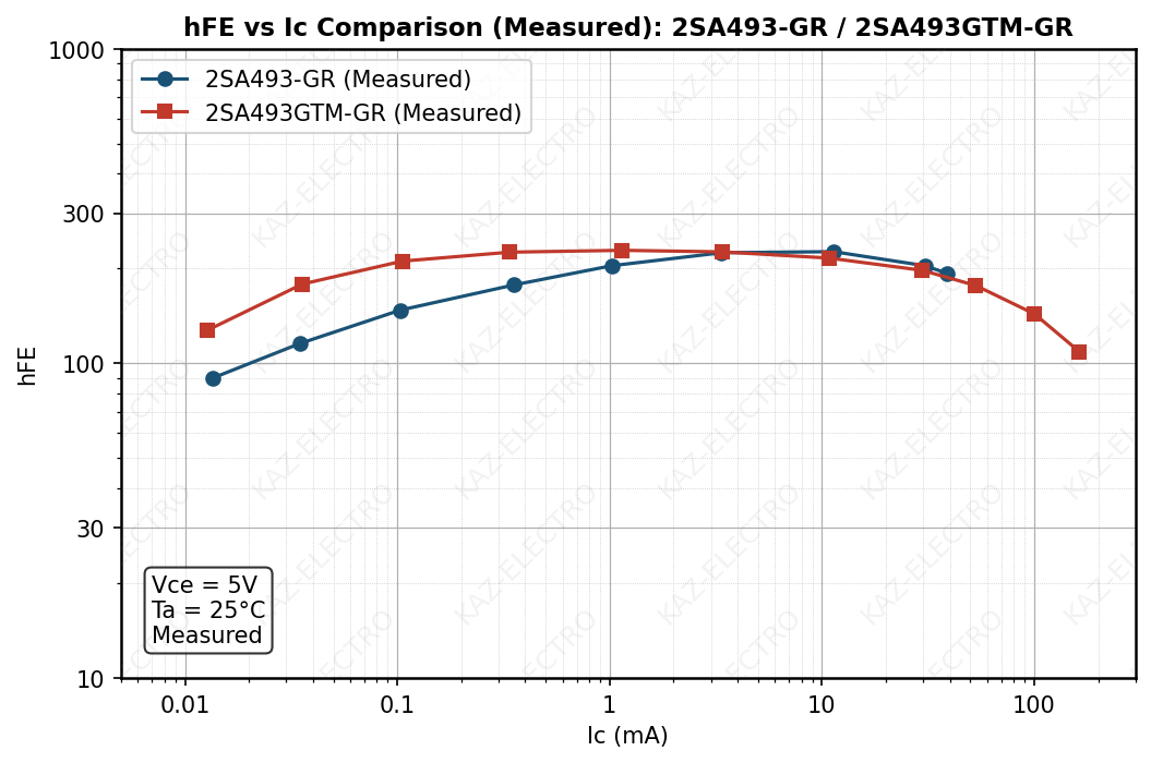
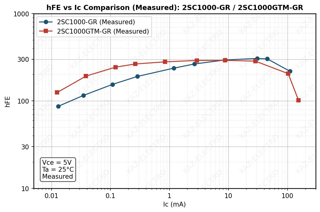
PNP side (2SA493): The absolute values are not dramatically different between TO-98 (original) and TO-92 (GTM), but the TO-92 (GTM) shows higher hFE at low currents and a flatter characteristic across a wider current range.
NPN side (2SC1000): Similarly, the TO-92 (GTM) shows higher hFE at low currents with a flat profile. The TO-98 (original) exhibits a hump-shaped characteristic peaking around 30–50 mA.
11.5.2 Normalized Comparison
Since absolute hFE values are subject to individual and rank variation, normalized graphs (value at 10 mA = 1.0) are used to compare curve shape.
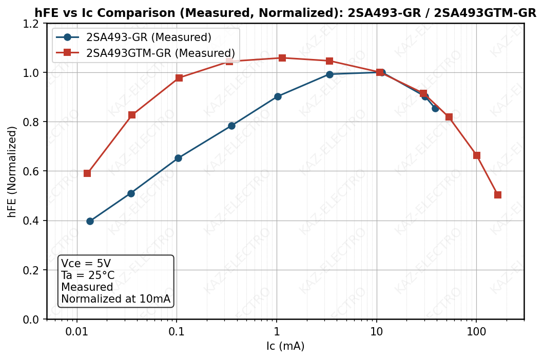
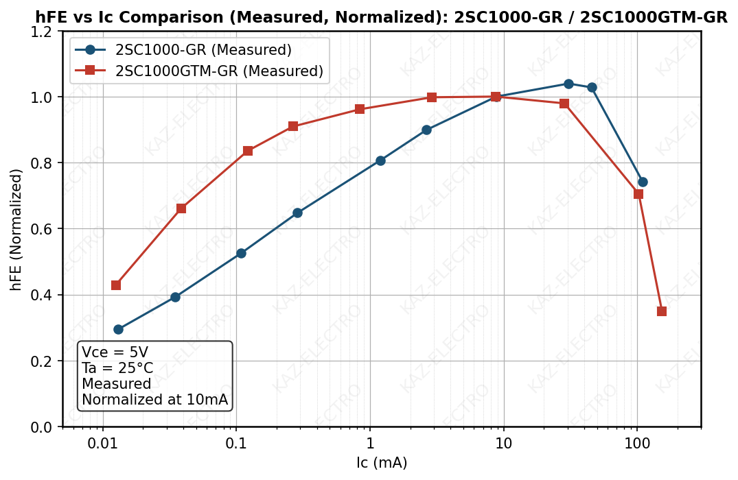
The normalized graphs make the design philosophies of the TO-98 (original) and TO-92 (GTM) clearly distinguishable:
- TO-98 (original): “high-hFE peak type” — peaks in the mid-to-high current range
- TO-92 (GTM): “wide-current flat type” — stable gain from low through high current
As noted earlier, low-noise transistors typically operate in the 0.1 mA to several mA range. The flat characteristic of the TO-92 (GTM) is well suited to this low-current operating regime.
11.6 VAF (Measured)
The Early voltage VAF is a parameter that directly governs output impedance (output conductance) and influences amplifier gain and PSRR (power supply rejection ratio). The following values were obtained using the author’s custom SPICE parameter analyzer.
| Polarity | Device | Package | VAF |
|---|---|---|---|
| PNP | 2SA493-GR | TO-98 | 56 V |
| PNP | 2SA493GTM-GR | TO-92 | 61 V |
| NPN | 2SC1000-GR | TO-98 | 165 V |
| NPN | 2SC1000GTM-GR | TO-92 | 293 V |
PNP side (2SA493): A slight increase from TO-98 (56 V) to TO-92 (61 V). No significant difference.
NPN side (2SC1000): A substantial improvement from TO-98 (165 V) to TO-92 (293 V). A higher VAF implies higher output impedance, which contributes to improved amplifier gain.
11.7 fT and Cob Characteristics (Measured)
The following values were obtained using the author’s custom fT meter and Cob meter. As noted above, no official Toshiba fT or Cob data exist for the 2SA493; the 2SA493G datebook values — whose die is presumed identical, as discussed in Chapter 4 — are used as the reference.
| Polarity | Device | Package | Cob @ Vcb = 5.6 V | fT @ Ic = 1 mA, Vce = 5 V |
|---|---|---|---|---|
| PNP | 2SA493-GR | TO-98 | 3.7 pF | 95 MHz |
| PNP | 2SA493GTM-GR | TO-92 | 3.6 pF | 100 MHz |
| NPN | 2SC1000-GR | TO-98 | 2.6 pF | 120 MHz |
| NPN | 2SC1000GTM-GR | TO-92 | 2.3 pF | 100 MHz |
No statistically significant difference attributable to the package change (TO-98 vs. TO-92) was observed.
The 2SA493G/2SC1000 series, across PNP/NPN and both TO-98 and TO-92 variants, carries a typical specification of Cob = 6 pF and fT = 80 MHz in the datasheets. The measured values obtained in this survey were generally better than these typical figures.
That said, transistor parameters such as fT and Cob inherently carry statistical spread, as does hFE. Depending on operating conditions, device generation, and lot characteristics, the spread between minimum and maximum can exceed a factor of two.
The author also standardized measurement conditions across PNP and NPN to ensure a fair comparison — which meant evaluating the PNP 2SA493 at the same low-voltage conditions used for the NPN, a slightly demanding condition for the PNP device. Taking this into account, the PNP/NPN differences observed here fall within a range the author considers acceptably small. On balance, the author concludes that no significant difference suggesting a die redesign was found between the TO-98 and TO-92 variants.
11.8 Discussion: Was the Die Changed?
Transistor parameters carry enough statistical spread to make definitive conclusions difficult, but within the scope of the author’s measurements, the following tendencies were observed:
| Parameter | TO-98 → TO-92 | Interpretation |
|---|---|---|
| hFE–Ic shape | Changed | Possible improvement in emitter concentration profile or surface treatment |
| VAF (PNP) | Slight increase | No significant change |
| VAF (NPN) | Substantial increase | Possible optimization of base doping profile |
| Cob | Nearly unchanged | Collector junction area (≈ die size) likely maintained |
| fT | Nearly unchanged | Basic structure (base width, etc.) likely maintained |
The fact that Cob and fT are essentially unchanged suggests that die size and fundamental structure were most likely preserved. On the other hand, the substantial VAF improvement on the NPN side suggests optimization of the base doping profile, and the change in hFE–Ic shape — specifically the suppression of hFE roll-off at high currents — hints at improvements to emitter dopant concentration profile or surface passivation.
11.9 Theoretical Supplement: Parameter Independence and Diagnostic Value
When assessing die identity, the diagnostic power of each parameter depends on its sensitivity to die structure versus its sensitivity to hFE. The table below summarizes the relevant characteristics.
Key parameter equations:
hFE–Ic shape: Governed by parameters such as emitter dopant concentration profile and surface recombination velocity — all process-dependent. Devices selected from the same die should share the same normalized curve shape even if absolute hFE values differ.
Early voltage VAF: VAF = QB / Cob ∝ (total base dopant) / (collector junction area). Governed by base doping profile and collector junction area; independent of hFE rank selection. A strong indicator of die identity.
Collector output capacitance Cob: Cob = Aj × √(εs × q × NC / 2(Vbi + VCB)), where Aj is junction area and NC is collector dopant concentration. Proportional to die size (junction area); unaffected by hFE rank selection. Devices from the same die should share the same Cob.
Transition frequency fT: fT = gm / (2π × Cπ) ≈ IC / (2π × VT × Cπ). Cπ depends on base width; fT is correlated with hFE but dominated by die structure. Individual spread is large, so fT alone is not sufficient for conclusions.
| Parameter | Die structure dependence | hFE dependence | Measurement precision | Diagnostic value |
|---|---|---|---|---|
| hFE–Ic shape | Good: emitter profile, process | — | High | Good |
| VAF | Excellent: base doping | None | Moderate (slope-based) | Excellent |
| Cob | Excellent: junction area | None | High | Excellent |
| fT | Good: base width | Moderate: correlated | Moderate (large individual spread) | Good |
11.10 Summary: The True Nature of the Transition from TO-98 (Original) to TO-92 (GTM)
Taken together, the measured data lead the author to the following interpretation of the TO-98 to TO-92 transition:
| Observation | TO-98 → TO-92 | Interpretation |
|---|---|---|
| hFE–Ic shape | Changed | Process improvement |
| VAF (NPN) | Substantially higher | Doping profile optimization |
| Cob | Nearly unchanged | Die size likely preserved |
| fT | Nearly unchanged | Basic structure likely preserved |
| Pc (max) | 0.2 W → 0.4 W | Improved thermal resistance via TO-92 transfer mold |
| Ic (max) | 50/100 mA → 150 mA | Possible use of heavier bonding wire |
A clear difference in hFE–Ic shape was confirmed — from “high-hFE peak type” (TO-98 original) to “wide-current flat type” (TO-92 GTM) — consistent with some change in manufacturing process. The substantial NPN VAF improvement reinforces this tendency.
At the same time, Cob and fT are nearly equivalent between the original and GTM types. Taken in isolation, this would suggest “the die was not changed.” But as the rating change table in Section 10.5.3 shows, the improvements in Pc, Ic, and breakdown voltage for this family are notably larger than for other TM-converted devices — a scale that is difficult to attribute to a package change alone. The further observation that the GTM’s characteristic curves bear a resemblance to those of the 2SA1015/2SC1815 adds one more point that cannot be dismissed.
In the end, whether the die was changed cannot be resolved from the measured data in this chapter. Cob and fT suggest the die was maintained; the rating increases and the altered hFE curve suggest changes to both die and process. The evidence on both sides is balanced, and no conclusion is possible at this time.
Answering this question would require a precise SPICE parameter comparison between the two types using measured data. The author regards this as a subject for future work and will not pursue the details here.
[Chapter 11 Summary] In the transition from TO-98 (original) to TO-92 (GTM), a clear difference in hFE–Ic shape was confirmed — from “high-hFE peak type” to “wide-current flat type” — consistent with some change in manufacturing process. However, Cob and fT are nearly identical, leaving the question of whether the die itself was changed unresolved from the measured data alone. The substantial rating increases (see Section 10.5.3) and the characteristic similarity to the 2SA1015/2SC1815 remain as grounds that cannot fully exclude a die change. A precise SPICE parameter comparison is left for future work.
12. Questions This Family Left Behind: Between the Record and Reality
Sixteen official Toshiba publications spanning 1966 to 2005, and accumulated observation notes on physical specimens — even with this body of primary source material, this family leaves behind questions that resist a definitive answer. This chapter gathers the “inconsistencies” encountered throughout the article, takes stock of the current state of the author’s thinking, and outlines what remains to be investigated.
12.1 The Map of Evidence — What the Datebook Record Shows and What Physical Specimens Reveal
Before listing the unresolved questions, the author summarizes the evidence accumulated throughout this article in a single table. Two types of row appear: ■ blue rows for official Toshiba datebook (hereafter “DB”) records, and ■ yellow rows for what physical specimens show. The gap between these two is what gives rise to most of the questions discussed below. Device designations in the specimen rows link to photographs; DB entries link to the master listing table in Section 9.4.4.
| Year / Period | Type | 2SA493/2SC1000 (original) |
2SA493G/2SC1000G (G type) |
2SA493GTM/2SC1000GTM (GTM type) |
2SC1000TM (TM type) |
|---|---|---|---|---|---|
| Dec. 1969 (est.) | Specimen | 2SC1000-BL katakana lot mark “エ” |
— | — | — |
| 1971 DB (Toshiba Semiconductor Handbook, Oct. 1970) |
Official record | — (not listed) | — | — | — |
| 1971 Handbook (Toshiba Electron Tube / Semiconductor / IC Handy Book) |
Official record | 2SA493: O/Y/GR 2SC1000: Y/GR/BL ※ 2SC1000 Y rank present (removed in 1973 DB) |
— (G type not yet present) | — | — |
| Mar. 1972 (est.) | Specimen | 2SA493-Y lot mark “マ” |
— | — | — |
| 1973 DB (Nov. 1972) |
Official record | O/Y/GR; GR/BL | Y/GR; GR/BL | — | — |
| 1975 DB (Nov. 1974) |
Official record | Y/GR; GR/BL | Y/GR; GR/BL | — | — |
| Feb. 1976 | Specimen | — | 2SA493G-BL datebook record and actual production: which came first? lot “6B” |
— | — |
| 1977 DB (Sep. 1976) |
Official record | NRND (Apr. 1976) |
GR/BL (Y dropped, BL added) |
— (not listed) | — |
| Oct. 1978 | Specimen | — | GR/BL (production continues) | 2SA493GTM-BL physically present despite DB absence lot “8J” |
— |
| 1978–1979 | Gap period | — | — | Physical specimens exist; absent from DB for ~2 years | — |
| 1980 DB (Jan. 1980) |
Official record | NRND continues | NRND | Y/GR no BL — first DB appearance ← rank regression |
First appearance in NRND/DISCON list |
| Oct. 1980 / Jan. 1982 | Specimen | — | — | — | 2SC1000TM-GR (1980.10, lot “0J”) 2SC1000TM-BL (1982.01, lot “2A”) |
| c. 1981 | Observation (inferred from other devices) | TO-98 phased out | TO-98 phased out | Y/GR (TO-92 primary production) | — |
| 1983 DB (Aug. 1983) |
Official record | DISCON → absent from all subsequent lists (reason unknown) |
DISCON | Y/GR (production continues) | DISCON |
| 1988 DB (Sep. 1988) |
Official record | — (absent from list) | DISCON | NRND (Sep. 1988) |
DISCON |
| Jan. 1991 | Specimen | — | — | 2SA493GTM-Y production continues 3 years after NRND designation; lot “1A” |
— |
| 2005 DB (small-signal SMD, final confirmed) |
Official record | — (absent from list) | DISCON | DISCON | DISCON |
Sources: TOSHIBA Semiconductor Handbook 1973/1975/1977; TOSHIBA Semiconductor Databook 1980/1983/1986; Toshiba Small-Signal Transistors Databook 1988; Power Transistor Databook 1990/1999; Small-Signal Transistors SMD 2005; and the author’s own specimen observation records. See Section 9.4.4 for detail.
Arranging the DB rows (blue) and the specimen rows (yellow) in chronological order makes visible a recurring gap between the official record and actual supply. The questions this gap raises are organized below by theme.
12.2 Mysteries of the Product History
12.2.1 Why did the 2SA493 (unmarked) disappear from the datebooks?
From 1983 onward, the 2SA493 (unmarked original type) is absent from the NRND/DISCON product lists in every Toshiba datebook — while the 2SC1000 (also original type), the 2SA493G, and the 2SA493GTM are all present (see Section 9.4.2).
In every datebook the author has reviewed, from the 1983 edition through the 2005 edition — five volumes in total — the 2SA493 (unmarked) does not appear. An absence spanning more than 20 years. Whether this reflects a simple editorial omission or something more deliberate remains unresolved at the time of writing.
12.2.2 When did volume production begin? — Three possibilities
Three possibilities for the start of volume production emerge from primary sources and physical specimens (see Section 7.1.1):
- Before 1969: the earliest specimen in the author’s collection (estimated December 1969, katakana lot mark “エ”)
- 1971: the year the device first appeared in Toshiba’s own Handy Book and in CQ Publishing’s 『最新トランジスタ互換表』 (CQ Publishing, 1971)
- 1972: the year of first listing in the 『1973 東芝半導体ハンドブック』 (Toshiba, November 1972)
“Around 1971” appears the most defensible working assumption at this time, but the extent of pre-1969 distribution remains unknown.
12.2.3 Why did the PNP type go NRND three years before the NPN?
The 2SA493 (unmarked) received its NRND designation in 1976. Its complementary partner, the 2SC1000, did not follow until 1979. Same family, same package — yet the PNP stepped back from the market three years earlier.
The competitive intensification of the consumer audio market and the asymmetric pressure created by The Four Technical Hurdles (see Chapter 7) are likely background factors. Combined with the fact that the 2SC1000 received a TM variant while the 2SA493 did not, the picture that emerges is one where the PNP side served primarily the consumer audio market and lost its rationale as new products arrived — making a TM transition unnecessary (see Section 6.4).
12.3 Gaps Between Datebook Record and Reality
12.3.1 Why did the GTM-BL exist two years before its datebook debut?
The 2SA493GTM first appeared in the 1980 datebook with only a Y/GR two-rank configuration — no BL rank was listed. Yet the author holds a 2SA493GTM-BL specimen dated October 1978 (No.60).
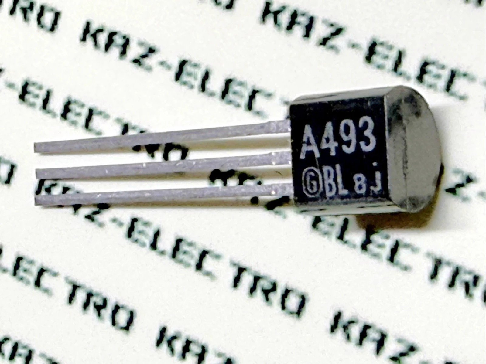
During this period, the 2SA493G — which was still in parallel production — carried a BL rank. The author’s reading is that during the TO-92 transition period, BL-rank specimens emerged from the same selection process used for the G type and were shipped as TM devices.
12.3.2 Why did production continue for three years after the NRND designation?
The 2SA493GTM received its NRND designation in September 1988. Yet the author holds a specimen with a production lot mark dated January 1991 (see Section 5.4, Figs. 5-1a/5-1b). This suggests that repair-parts supply through Toshiba’s service network continued for some time after the catalog-level NRND designation took effect.
This kind of gap between “end of datebook record” and “end of actual production” is not unique to this family. The 2SC1000TM, discussed in Section 6.1, also has documented production after its DISCON designation. The terms “NRND” and “DISCON” as used in practice at that time may not have carried the same precision as today’s NRND/EOL/DISCON designations.
12.3.3 Replacement designations that vary by source — 2SA970 or 2SA1015?
The replacement designation for the 2SA493GTM alternates between 2SA970 and 2SA1015 depending on the source (see Section 9.4.3).
As a low-noise transistor, the 2SA970 is the natural technical successor to the 2SA493GTM. Yet the general-purpose small-signal 2SA1015 appears as the designated replacement in multiple datebook editions. Whether Toshiba took the view that the 2SA1015 was sufficient from an NF perspective, or whether the variation simply reflects differences between editors or editions, cannot be determined at this time.
12.4 Mysteries of Manufacturing
12.4.1 Reading the hFE rank transitions
The hFE rank configuration of this family changed multiple times across generations. The history of PNP high-hFE manufacturing difficulty and process improvement is embedded in those changes. The author’s reading, organized chronologically:
- 2SC1000-Y (early production): Even the GR rank of the 2SA493 (PNP) was initially difficult to yield. The NPN side offered a Y rank — a low-hFE product — to allow the complementary pair to exist as a viable matched set.
- 2SC1000-Y discontinued: Process improvements raised the 2SA493-GR yield. The NPN no longer needed to “come down” to meet the PNP, and the Y rank disappeared.
- 2SA493-O discontinued: As the process stabilized, the hFE distribution shifted upward. The low-hFE O rank became naturally unnecessary.
- 2SA493G-O never introduced: For telecom/industrial applications, requirements were more demanding from the outset; low-gain devices were never part of the lineup.
- 2SA493G-BL added: As PNP high-hFE yield became achievable through late-1970s process improvements, the BL rank was added to the lineup in the 1977 datebook.
- 2SA493GTM-BL (early TM phase): Around 1978, TO-98 production began transitioning to TM packaging, carrying the 2SA493G-BL designation into the TM format. The physical existence of the GTM-BL specimen (Section 12.3.1) corroborates this.
- 2SA493GTM-Y/GR (rank regression): The GTM renewal brought substantial specification and rating changes. Under the new specifications, high-hFE PNP production became difficult to yield consistently once again, and the lineup settled back to the same Y/GR two-rank configuration seen in the 1973 datebook for the 2SA493G/2SC1000G.
Surveying these hFE rank transitions across the full family timeline, the 1980 GTM configuration is a striking echo of the 1973 G configuration — a kind of rank regression across generations.
Reference: When a high-hFE complementary pair is needed
Stable supply of high-hFE PNP devices was a manufacturing challenge shared across the industry, not unique to this family. The following table lists contemporary low-noise high-hFE complementary pairs by manufacturer. All are discontinued as of 2025. See also the equivalent device table in Chapter 13.
| Manufacturer | PNP | NPN | hFE range |
|---|---|---|---|
| Toshiba | 2SA970-BL | 2SC2240-BL | 350–700 |
| NEC | 2SA990-E | 2SC1843-E | 400–800 |
| Sanyo | 2SA1391-U | 2SC3392-U | 280–560 |
| Matsushita | 2SA1127-T | 2SC2634-T | 360–700 |
| Hitachi | 2SA1083-E | 2SC2545-E | 400–800 |
| Mitsubishi | 2SA999L-F | 2SC2320L-F | 250–500 |
※ All discontinued as of 2025. NEC’s discrete device business contracted significantly following the integration into Renesas Technology, and many notable devices disappeared.
12.4.2 PNP fT and Cob absent from the 1973 datebook
As noted in the ratings table in Section 3.2, the 1973 datebook entry for the 2SA493 (PNP) carries no values for fT or Cob — even though the complementary 2SC1000 does.
The manufacturing difficulties specific to PNP devices (see Section 8.2) likely contributed to characteristic instability that may have made publication impractical. Whether this was a deliberate non-disclosure or a constraint of measurement technology at the time remains unclear.
12.4.3 Why does the narrow font appear only on certain devices?
The marking style evolution of TO-98 packages, touched on in Section 1.3, identifies the narrow font as a feature of the later production period. Specifically, it appears prominently on the last TO-98 devices introduced: the 2SA841/2SC1681 and 2SA842/2SC1682. Not all contemporaneous devices made the switch, however.
Whether this reflects differences between production lines, lot-to-lot variation, or the timing of equipment changeovers — the author’s specimen observations alone do not yield a conclusion.
12.4.4 The meaning of the X mark remains unresolved
On the X-mark specimens observed in Section 10.4, the origin remains unexplained. The following are established from observation: “not seen on early specimens from the hiragana/katakana lot-mark era”; “disappears from resin-package devices in the 1980s and later”; “continues to appear occasionally on metal-can package devices into later periods.” What accounts for this pattern of appearance and disappearance is still in the realm of inference. If any reader has knowledge of what the X mark signifies, the author would very much like to hear from them.
12.5 Ongoing Research
The following items have accumulated observation data, but have not yet reached a conclusion. The author intends to take them up in a future separate article or in a later revision of this article.
- The complete picture of lot marking rules — the transition boundaries from lowercase Roman letters → hiragana → katakana → alphanumeric, and the exceptions to those rules, are under continued observation across thousands of physical specimens.
- The shared selection process for 2SA493GTM-BL and 2SA493G-BL — how BL-rank devices were produced during the transition period. This is difficult to confirm without internal documentation.
- The true reason for the 2SA493 (unmarked) absence from datebook lists — editorial error or deliberate handling?
- Why Pc doubled (0.2 W → 0.4 W) in the TO-92 transition — separating the individual contributions of lead frame material changes, heavier bonding wire, and improved thermal resistance through transfer molding. The data to isolate these factors are not yet in hand.
[Chapter 12 Summary] This chapter organized the questions that have accumulated through datebook records and physical specimen observation: the disappearance of a device designation from the listings, the evolution of hFE rank configurations, the existence of unlisted devices, the mystery of the X mark — none reaching a firm conclusion, but the observational evidence continues to accumulate. Without the help of Toshiba personnel who were present at the time, fully resolving all of these may prove difficult. The author intends to keep investigating.
→ Next chapter: equivalent and replacement device information.
13. Equivalent & Replacement Guide
This chapter provides a practical cross-reference guide for 2SA493/2SC1000 equivalents and replacements, compiled from Toshiba, Sony, and CQ Publishing sources — intended as a reference for restorers and repair enthusiasts worldwide.
13.1 Equivalent Device Information
The following represents the results of the author’s research into equivalent device information from semiconductor manufacturer datebooks and published references. In international markets, restorers and repair enthusiasts typically search using the keywords “equivalent” or “replacement.” The author hopes this chapter serves as a useful practical reference in those searches.
13.1.1 Research methodology
Low-noise transistors fall into two broad categories: high-voltage and medium/low-voltage types, which can differ in their operating character. The 2SA493/2SC1000 is a medium-voltage (VCEO approximately 50 V) complementary pair; the author therefore focused primarily on low-noise complementary pairs of similar voltage rating.
13.1.2 Sources
This table draws on four categories of information: Toshiba’s own successor device designations; general equivalent information from CQ Publishing’s transistor cross-reference publications; information from Sony’s SONY補修用半導体ハンドブック (Sony, 1981/1982/1994); and the author’s own recommendations.
Sony, as a major integrated electronics manufacturer, has historically used a wide range of semiconductors. Equivalent data that Sony’s service technicians referenced for repairing Sony products is considered useful for enthusiasts attempting repairs on Sony equipment, and has therefore been included.
To make this provenance immediately readable, the table includes a “Recommended by” column identifying the source of each equivalent suggestion.
13.1.3 Usability and practical design
The 2SA493/2SC1000 is a complementary pair, but different sources do not necessarily recommend complete complementary replacements. For example, Sony recommends the 2SC1362 as a replacement for the 2SC1000, but does not list the 2SC1362’s complementary counterpart 2SA705 as a replacement for the 2SA493. This type of single-polarity recommendation is common in general-purpose cross-reference publications from CQ Publishing as well.
To address this, the author has included both the PNP and NPN device wherever a source recommends only one polarity, giving readers a more complete basis for exploring replacements.
A further note: Toshiba itself, in the 1980 datebook, designated the 40 V-rated 2SA842 as a replacement for the 50 V-rated 2SA493 — an example of the voltage-rating mismatch that was a recurring risk in period equivalent recommendations. Wherever this occurs in the table, a “⚠ VCEO caution” note has been added.
A note on period equivalent selection practices
In the design environment of the time, a certain body of experience-based reasoning operated alongside — and sometimes at variance with — catalog specifications: confidence that quality devices carried margin well beyond their published ratings; the assumption that well-designed circuits would not stress components to their maximum ratings; and the practical reality that nominal 50 V devices might begin to show elevated Ic in the region below breakdown. These background factors shaped period equivalent selections in ways that catalog data alone do not capture. The author recommends reading period equivalent information with this context in mind — datasheet limits were not always treated as absolute.
The author has added individual “⚠ VCEO caution” notes for entries where the equivalent device carries a lower breakdown voltage than the original. All CQ Publishing and Toshiba equivalent data are reproduced as originally published, including entries the author considers open to re-examination — preserving the historical record as-is is the intent of this archive.
Readers are asked to check the “Recommended by” column, any cautionary notes, and the rated parameters before applying any of the information in this table.
[Note] Early replacement designations contained voltage-rating mismatches. The 1977 datebook designated the 2SA842 (VCEO = 40 V) as a replacement for the 2SA493 (VCEO = 50 V); from the 1980 datebook onward, this was corrected to the 2SA970 (VCEO = 120 V). Always verify VCEO when selecting replacement devices.
Important: Disclaimer and safety notice
The equivalent device information presented here is based solely on a survey of catalog specifications from semiconductor manufacturers. No operational testing or functional verification on actual equipment has been performed.
Transistor substitution is an action that can lead to equipment failure or performance degradation. The information on this site is provided for reference only. The author accepts no responsibility for any damage arising from substitution work carried out based on this information.
When attempting any substitution, consider not only the maximum ratings shown in the table (VCEO, IC, PC) but also parameters with direct impact on circuit operation — particularly fT (transition frequency) and Cob (output capacitance). Always select replacements based on your own judgment of the voltage ratings and characteristics involved, and proceed entirely at your own risk.
Low-Noise Transistor Equivalent / Replacement / Cross-Reference Table
| Device | Manufacturer | Vceo (V) |
Ic (A) |
Pc (W) |
NF | hFE | fT (MHz) |
Cob (pF) |
Recommended by | Notes |
|---|---|---|---|---|---|---|---|---|---|---|
| 2SA493/2SC1000 (1975) |
Toshiba | −50/50 | −0.05/0.1 | 0.2/0.2 | <2/<3 (120 Hz/100 Hz) |
70–400/ 200–700 |
—/80 | —/6 | — | Original type (TO-98) |
| 2SA493G/2SC1000G (1977) |
Toshiba | −50/50 | −0.05/0.1 | 0.2/0.2 | <2/<2 (120 Hz/100 Hz) |
200–700/ 200–700 |
80/80 | 6/6 | — | Industrial grade (TO-98) |
| 2SA493GTM/2SC1000GTM | Toshiba | −50/50 | −0.15/0.15 | 0.4/0.4 | <2/<2 (100 Hz) |
120–400/ 200–700 |
80/80 | 6/6 | Toshiba · CQ · Kaz | New industrial type (TO-92) |
| 2SA970/2SC2240 | Toshiba | −120/120 | −0.1/0.1 | 0.3/0.3 | <2 (1 kHz) | 200–700/ 200–700 |
100/100 | 4.0/3.0 | Toshiba · CQ · Kaz | |
| 2SA640/2SC1222 | NEC | −45/50 | −0.05/0.1 | 0.25/0.25 | <4/<3 (100 Hz) |
100–700/ 225–1000 |
100/100 | 8.0/3.5 | CQ | CQ recommends 2SA640 only; NV <30/<30 mV |
| 2SA672 | Hitachi | −50 | −0.2 | 0.2 | 1.6 (freq. unspecified) | 60–320 | 105 | 16 | CQ | |
| 2SA705/2SC1362 | Sony | −50/50 | −0.2/0.2 | 0.32/0.32 | —/<6 (1 kHz) |
129–690/ 129–690 |
—/— | 6.0/4.5 | Sony | Sony recommends 2SC1362 only; proprietary package |
| 2SA722/2SC1328 | Matsushita | −55/55 | −0.05/0.05 | 0.4/0.4 | Nv <150 mV | 180–700/ 180–700 |
—/— | —/— | Kaz | |
| 2SA725/2SC1312 | Mitsubishi | −35/35 | −0.1/0.1 | 0.2/0.2 | 0.5/0.5 (1 kHz) |
250–1200/ 250–1200 |
100/150 | 3/2.5 | CQ | CQ recommends 2SC1312 only; ⚠ VCEO caution. High-voltage version: 2SA726/2SC1313 |
| 2SA726/2SC1313 | Mitsubishi | −50/50 | −0.1/0.1 | 0.2/0.2 | 0.5/0.5 (1 kHz) |
250–1200/ 250–800 |
100/150 | 3/2.5 | Kaz | Nv <300/<300 mV |
| 2SA750/2SC1400 | NEC | −50/80 | −0.05/0.05 | 0.25/0.25 | <3/<3 (100 Hz) |
225–1000 | 100/100 | 6.5/2.7 | Kaz | Nv <25/<30 mV |
| 2SA836/2SC1345 | Hitachi | −55/50 | −0.1/0.1 | 0.2/0.2 | <1/<1 (1 kHz) |
160–500/ 250–1200 |
200/230 | 2.0/<3.5 | CQ · Kaz | |
| 2SA841/2SC1681 | Toshiba | −60/60 | −0.05/0.05 | 0.2/0.2 | <1/<1 (1 kHz) |
200–700/ 200–1200 |
140/130 | 4.5/2.6 | Kaz | |
| 2SA842/2SC1682 | Toshiba | −40/40 | −0.05/— | 0.2/0.2 | <3/<3 (1 kHz) |
200–700/ 200–1200 |
140/130 | 4.5/2.6 | Toshiba | Toshiba recommends 2SA842 only; ⚠ VCEO caution |
| 2SA930/2SC1570 | Sanyo | −50/50 | −0.05/0.1 | 0.2/0.2 | VNO 35 mV | 160–960/ 160–960 |
80/100 | 5/3 | Kaz | |
| 2SA990/2SC1843 | NEC | −50/50 | −0.1/0.1 | 0.25/0.25 | NV <40/<40 mV | 200–800/ 200–800 |
180/100 | 4.5/3.0 | Kaz | |
| 2SA991/2SC1844 | NEC | −60/60 | −0.1/0.1 | 0.5/0.5 | NV <45/<45 mV | 200–800/ 200–800 |
90/100 | 5.5/4.8 | Kaz | en 0.55/0.6 nV/√Hz |
| 2SA999L/2SC2320L | Mitsubishi | −50/50 | −0.2/0.2 | 0.3/0.3 | 0.5/0.5 (1 kHz) |
150–500/ 150–500 |
200/200 | 7.0/3.5 | Kaz | |
| 2SA1015/2SC1815 | Toshiba | −50/50 | −0.15/0.15 | 0.4/0.4 | —/— | 70–400/ 70–700 |
>80/>80 | 4.0/2.0 | CQ · Kaz | |
| 2SA1015L/2SC1815L | Toshiba | −50/50 | −0.15/0.15 | 0.4/0.4 | <6/<6 (100 Hz) |
70–400/ 70–700 |
>80/>80 | 4.0/2.0 | Kaz | Noise-controlled grade |
| 2SC1032/2SC2310 | Hitachi | −50/50 | −0.1/0.1 | 0.2/0.2 | <5/— (120 Hz) |
100–320/ 250–1200 |
280/230 | 3.3/1.8 | Kaz | Lower-voltage variant: 2SA1031/2SC458LG |
| 2SA1027R | Mitsubishi | −50 | −0.2 | 0.25 | 0.7 (1 kHz) | 300 | 100 | 6.5 | Sony | Not listed in Mitsubishi datebooks |
| 2SA1083/2SC2545 | Hitachi | −60/60 | −0.1/0.1 | 0.4/0.4 | en <0.5 nV/√Hz (1 kHz) |
250–800/ 250–1200 |
90/90 | 3.5/3.0 | Kaz | Higher-voltage variant: 2SA1084/2SC2546 |
| 2SA1100L/2SC2575L | Mitsubishi | −50/50 | −0.2/0.2 | 0.3/0.3 | 0.5/0.5 (1 kHz) |
150–500/ 150–800 |
200/200 | 7.0/3.5 | Kaz | Nv <150/<150 mV |
| 2SA1127/2SC2634 | Matsushita | −55/55 | −0.1/0.1 | 0.4/0.4 | NV <150 mV | 180–700/ 180–700 |
—/— | —/— | Kaz | |
| 2SA1175/2SC2785 | NEC | −50/50 | −0.1/0.1 | 0.25/0.25 | <20 (100 Hz) | 110–600/ 110–600 |
180/250 | 4.5/3.0 | Sony | Compact version of 2SA733/2SC945 |
| 2SA1391/2SC3392 | Sanyo | −120/120 | −0.05/0.05 | 0.3/0.3 | <0.8/0.8 (1 kHz) |
140–560/ 140–560 |
150/150 | 4/3 | Kaz | |
| 2SC900 | NEC | 35 | 0.1 | 0.25 | <4 (100 Hz) |
225–1000 | 100 | 3.5 | CQ | NV <40 mV; ⚠ VCEO caution |
| 2SC945L | NEC | 50 | 0.1 | 0.25 | <20 (100 Hz) | 90–600 | 250 | 3.5 | Kaz |
Sources: Toshiba — TOSHIBA Semiconductor Databook 1977/1980, Handbook 1983/1986, 東芝半導体ハンドブック 1966/1969/1971/1973/1975, Small-Signal Transistors SMD 2005 / NEC — 電子デバイスデータブック ’79 半導体編, ’83 トランジスタ編 / Hitachi — ’79 SEMICONDUCTOR DATA BOOK トランジスタ・ダイオード / Mitsubishi — ’80 半導体データブック トランジスタ 小信号ダイオード編, 1983–1984 / Matsushita — ’83 ナショナル半導体 ディスクリート半導体 / Sanyo — ’87–’88 半導体データブック 個別半導体素子トランジスタ編 / Sony — SONY補修用半導体ハンドブック 1981/1982/1994, ソニー半導体ハンドブック 1979 / Published references — 『トランジスタ規格表』 (CQ Publishing, 1968–1989); 『最新トランジスタ互換表』 (CQ Publishing, 1970–2003); 『初歩のラジオ トランジスタ・ハンドブック』 (Seibundo Shinkosha)
When selecting a replacement device, choosing the right device for the application is essential. For the safest choice, the 2SA970/2SC2240 pair remains the most defensible option. For those where availability is the primary constraint, the 2SA1015/2SC1815 (genuine Toshiba production) is a viable alternative.
→ Next chapter: conclusion and closing.
14. Reader Guide
[For Repair and Restoration Enthusiasts]
- As of 2025, original TO-98 specimens are extremely difficult to source.
- Toshiba’s designated replacement: 2SA970/2SC2240 (currently available as NOS).
- The NPN side (2SC2240) offers good drop-in compatibility. The PNP side (2SA970) has roughly twice the hFE of the original 2SA493, so bias adjustment is likely needed.
- The equivalent device table in Chapter 13 is available as a practical reference for replacement selection.
→ Everything you need to make that call is here.
[For Effects Builders and Pedal Makers]
- The 2SC1000-GR was used in the Roland AF-60 “Bee Gee Fuzz” and AD-50 “Double Beat.”
- The TO-98 era’s hFE–Ic characteristic — with its peak in the low-current range — may have contributed to the distinctive fuzz tone of those units.
- Modern replacements (such as the 2SC2240) carry a flat characteristic, which may produce audible tonal differences.
- If chasing that original sound is the goal, hunting down an original TO-98 unit or a GTM specimen is worth the effort.
→ The character of that tone may be hiding inside this curve.
[For Audio Engineers and Circuit Designers]
- The hFE–Ic characteristics of the original type and the G type are nearly identical — consistent with both being selected from the same die.
- The G type and GTM type show distinctly different curve shapes: from a mid-to-high-current peak type to a wide-range flat type.
- Cob and fT are essentially equivalent between the G type and GTM type.
- Measured data are presented in detail in Chapter 11.
→ The story behind the datebook numbers begins to come into focus.
[For Those Interested in Semiconductor and Technology History]
- PCT technology (completed in 1969) was the key to achieving low-noise performance in this family.
- Despite its low type number (2SA493), the device’s market debut was delayed — the background to that delay is documented in The Four Technical Hurdles (Chapter 7).
- Both devices received early NRND designations: the 2SA493 in 1976, the 2SC1000 in 1979. The consumer-market variants had short lives; only the industrial G Series remained in production into the early 1990s.
- The “TM” and “GTM” naming convention was a Toshiba-specific strategy — other manufacturers did not assign new type numbers for equivalent package transitions.
→ From a single transistor, an era becomes visible.
[For Collectors]
- Original TO-98 specimens are rare and difficult to obtain.
- Manufacturing period can be estimated from the lot mark and date code inscribed on the package (see the product history sections in Chapters 3–6).
- Devices not listed in any datebook — such as the 2SC1000TM — are known to exist in physical form (see Chapters 6 and 10).
- Cross-referencing a specimen against the information in this article can help establish the provenance of a piece in your own collection.
→ Behind the marking, someone’s work remains.
15. References
This chapter lists the primary sources, datebooks, and published references cited in this article.
| Publisher | Title | Year(s) |
|---|---|---|
| Toshiba | 東芝半導体ハンドブック (Toshiba Semiconductor Handbook) | 1969, 1971, 1973, 1975 |
| 東芝半導体ハンドブック3 (Toshiba Semiconductor Handbook Vol.3) | 1966 | |
| 東芝 電子管・半導体・集積回路 ハンディブック (Toshiba Electron Tube / Semiconductor / IC Handy Book) | 1967, 1971 | |
| 東芝半導体データブック | 1977, 1980, 1983, 1986 | |
| 東芝半導体製品総覧表 | 1982, 1988 | |
| パワートランジスタデータブック | 1990, 1999 | |
| 東芝 小信号トランジスタ SMD (Toshiba Small-Signal Transistors SMD) | 2005 | |
| NEC | NEC エレクトロニクス・データブック (NEC Electronics Databook) | 1969 |
| NEC 電子デバイス・データブック 半導体&IC (NEC Electronic Devices Databook: Semiconductors & ICs) | 1972 | |
| NEC 電子デバイス・データブック 半導体 (NEC Electronic Devices Databook: Semiconductors) | 1979 | |
| NEC 電子デバイス・データブック トランジスタ (NEC Electronic Devices Databook: Transistors) | 1983 | |
| Hitachi | 日立半導体ハンドブック (Hitachi Semiconductor Handbook) | 1967, 1969 |
| 日立 SEMICONDUCTOR DATA BOOK トランジスタ・ダイオード (Hitachi Semiconductor Data Book: Transistors & Diodes) | 1979 | |
| 日立トランジスタ・データブック (Hitachi Transistor Databook) | 1986 | |
| Mitsubishi | 三菱半導体ハンドブック トランジスタ&パワー半導体 (Mitsubishi Semiconductor Handbook: Transistors & Power Semiconductors) | 1976 |
| 三菱半導体データブック トランジスタ・小信号ダイオード (Mitsubishi Semiconductor Databook: Transistors & Small-Signal Diodes) | 1978, 1979, 1980 | |
| 三菱半導体データブック トランジスタ・小信号ダイオード・ハイブリッドIC・オプトエレクトロニクス (Mitsubishi Semiconductor Databook: Transistors, Small-Signal Diodes, Hybrid ICs & Optoelectronics) | 1983-1984 | |
| Matsushita | ナショナル半導体ハンドブック (National Semiconductor Handbook) | 1967, 1971, 1977 |
| ナショナル半導体ハンドブック ディスクリート半導体 (National Semiconductor Handbook: Discrete Semiconductors) | 1983 | |
| Sanyo | 三洋半導体データブック (Sanyo Semiconductor Databook) | 1971, 1976, 1981 |
| 三洋半導体データブック ディスクリートトランジスタ (Sanyo Semiconductor Databook: Discrete Transistors) | 1987-1988 | |
| Sony | SONY リペア用半導体ハンドブック (Sony Repair Parts Semiconductor Handbook) | 1981, 1982, 1994 |
| ソニー半導体ハンドブック (Sony Semiconductor Handbook) | 1979 | |
| CQ Publishing / Seibundo | CQ出版 トランジスタ規格表 (Transistor Spec Reference, CQ Publishing) | 1968–1989 (annual editions) |
| CQ出版 最新トランジスタ互換表 (Transistor Compatibility Reference, CQ Publishing) | 1970–2003 (annual editions) | |
| 誠文堂新光社 初歩のラジオ トランジスタ・ハンドブック (Beginner’s Radio: Transistor Handbook, Seibundo Shinkosha) | 1972 |