2SC1815 SPICE Parameter Measurement Report
Chapter 1 Why Measure It Yourself?
1-1 How I Came to Measure Everything Myself
Measuring SPICE parameters myself was never part of the original plan.
At first, I read values from databook graphs and typed them manually into the simulator. Printed datasheets smear and distort. Read-back accuracy has its limits, and fitting errors grow accordingly. Worse, the graphs never state whether the plotted data are nominal values or measured representative values.
As for Cib, Tstg, and hoe — the majority of devices never publish these figures at all. Parts that disclose every parameter needed for a complete model are, frankly, nonexistent.
All parameters are interconnected. Mixing databook figures with partial measurements of my own breaks the internal consistency of the model. Models that circulate in the world face the same problem — the bundled models that come with simulation software, the unattributed files found on the internet, none of them comes with any documented provenance.
The problem becomes clear when you look at an actual example. Here is what happens when you try to build a model by combining databook readings with partial measurements.
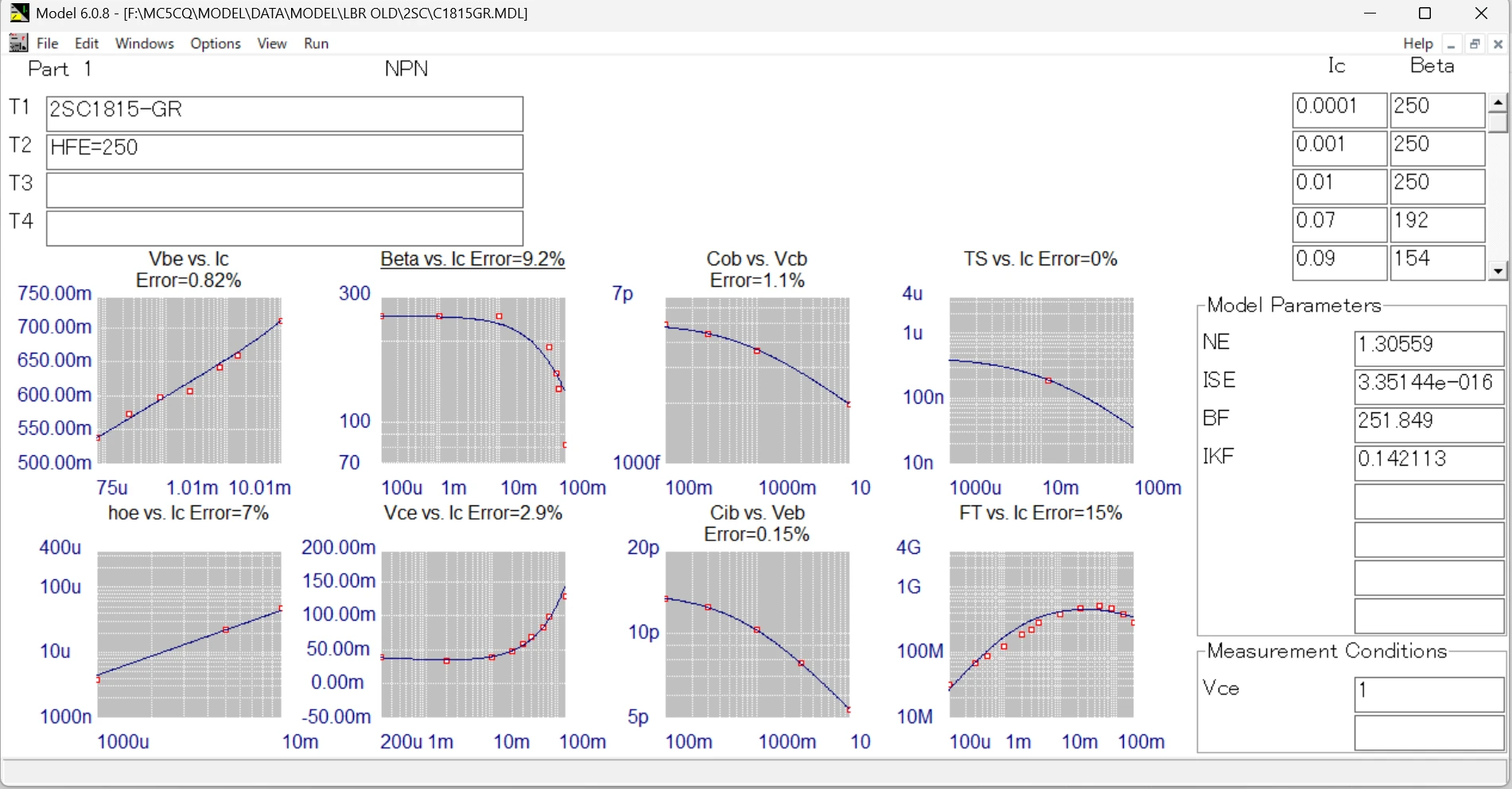
The fit error on Beta vs. Ic is 9.2%; fT vs. Ic, 15%; hoe vs. Ic, 7%. The curves are visibly offset from the measured points.
Even these results look relatively clean only because I took the time to read the log-scale graduations to the nearest 0.25 mm. If the reading conditions are even slightly worse, errors of 10–30% are not unusual. I have encountered cases where the datasheet graph itself appears to be wrong and the fit refuses to converge at all. My shift to measurement-first practice is the accumulated result of exactly that kind of bitter experience.
All of this led me to one conclusion: there is no substitute for measuring it yourself.
There are other motivations as well.
On weekday evenings, after dinner, I want to advance circuit design work without picking up a soldering iron. I want to organize my thinking at the desk before the weekend’s hands-on work. A trustworthy model makes that possible.
There is also the urge to swap models and explore. Swap out a transistor and the sound changes — I want to trace the reason through simulation. I want to reproduce hFE spread and thermal DC drift with measurement-grade accuracy. Rather than swapping base stop resistors in and out while watching the oscilloscope, I want to choose reasonable values from first principles — knowing RB and RBM in advance.
Parts that appear to share the same die despite different packages and part numbers — I want to verify that by looking inside. And above all, for parts where neither a datasheet nor a SPICE model is available, there is simply no way to know the characteristics except to measure them yourself.
These motivations accumulated until I built the measurement hardware and set to work extracting parameters from the 2SC1815.
1-2 hFE Rank Structure of the 2SC1815 and Reference Models for Comparison
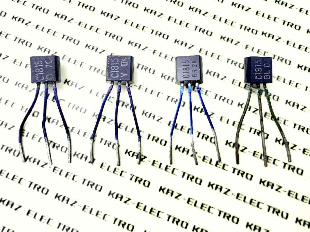
The 2SC1815 comes in four hFE ranks: O, Y, GR, and BL. O (70–140), Y (120–240), GR (200–400), BL (350–700) — a classification that divides a nearly decade-wide span, from a lower limit of 70 to an upper limit of 700, into four tiers.
There are many situations where simulating the effect of different hFE ranks becomes necessary. That has been my experience as well. For that reason, all four ranks were modeled this time.
Verifying the extraction results requires a reference to compare against. An official Toshiba SPICE model for the 2SC1815 would be ideal, but the part reached end-of-life in 2012–2013 and vanished before any official model was published. As of 2025, however, a SPICE model for the 2SC2712 — considered to share the same die in SMD form — is publicly available. That model serves as the reference for evaluating the modeling results here.
The rank to which the 2SC2712 model corresponds is not disclosed. The representative hFE–Ic curve in the datasheet shows a plateau peak of approximately 170, close to the midpoint of the Y-rank band (120–240). My interpretation is that Toshiba treated Y as the representative rank when establishing the nominal data.
Whether the 2SC2712 truly shares the same die as the 2SC1815 — including the question of its relationship with the 2SA1015 — will be examined in a separate article (2SA1015 / 2SC1815 — Japan’s Most Famous Complementary Pair). For this report, the comparison proceeds on the premise that the die is the same, and any parameter discrepancies encountered along the way are discussed as they arise.
The datasheet curves are published as common to all ranks, but in practice the characteristics differ substantially depending on whether the part on hand is an O or a GR. The following graph shows exactly that.
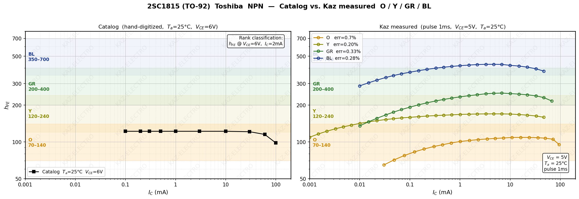
The datasheet curve (left panel) and the four Kaz-measured curves overlaid (right panel) are shown side by side. Which rank band the datasheet curve falls within can be read from the color-coded bands in the left panel.
Chapter 2 How the Measurements Were Made
2-1 Three Custom-Built Measurement Systems
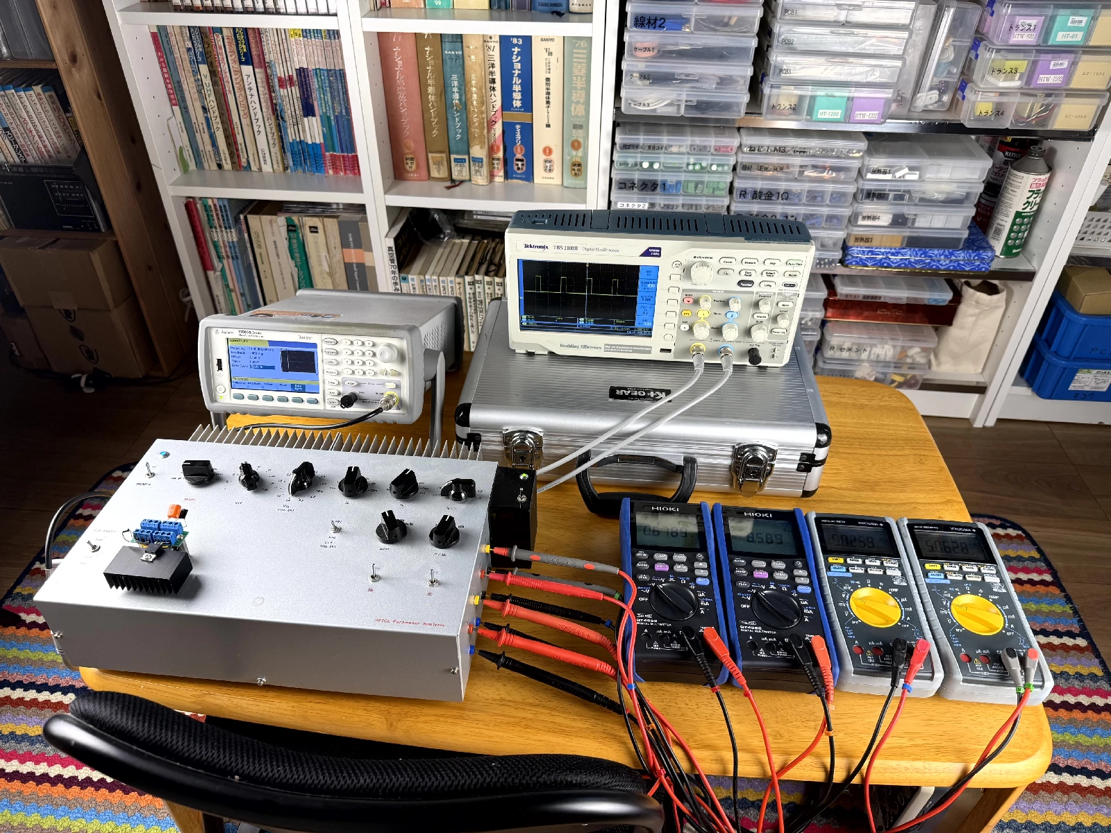
Three custom-built systems are used for the measurements. Key specifications are listed on the Reference Materials page, but a more detailed look at each system’s configuration follows here.
The design concept behind this instrument is unambiguous: eliminate self-heating error without compromise. A simple bench setup measures VBE and hFE by DC. At currents of around 1 mA, this causes no problems. Extracting SPICE parameters, however, requires sweeping current and voltage across a wide range — from the microamp region up to near the absolute maximum ratings. In DC measurement, self-heating of the device under test (DUT) becomes noticeable once IC exceeds roughly 10 mA, at which point VBE and hFE begin to drift into unrealistic territory. Once the DUT heats up, returning to room temperature takes more than 30 minutes. With dozens of data points to collect, this is simply unworkable.
There are even more serious cases. In small packages where no heatsink can be attached — yet the device handles large currents — continuing DC measurement with VCE applied while IC exceeds 0.1 A will outrun the device’s thermal dissipation capability and cause thermal failure. This is not a matter of DC measurement degrading accuracy; it is a case where DC measurement simply cannot be used.
The solution is to minimize the time current flows — pulse measurement mode. Adding pulse mode also enables the switching tests needed to derive TR. By observing the collector’s pulse response on an oscilloscope while driving the base with a pulse, Tstg, ton, and toff can be measured as well. These Tstg measurements are then fed into the software as the Ic vs. Tstg graph, from which the SPICE parameter TR is extracted.
The design philosophy settled early: use commercial instruments wherever they suffice. Building the signal source from scratch was considered initially, but fabricating everything from the ground up would take forever. That idea was abandoned quickly. An arbitrary waveform generator for the pulse reference voltage source, high-accuracy DMMs for current and voltage measurement, an oscilloscope for waveform monitoring — commercial instruments connected as peripherals, with the custom-built portion limited strictly to what is not available off the shelf. Build what cannot be bought; buy what can. A simple rule.
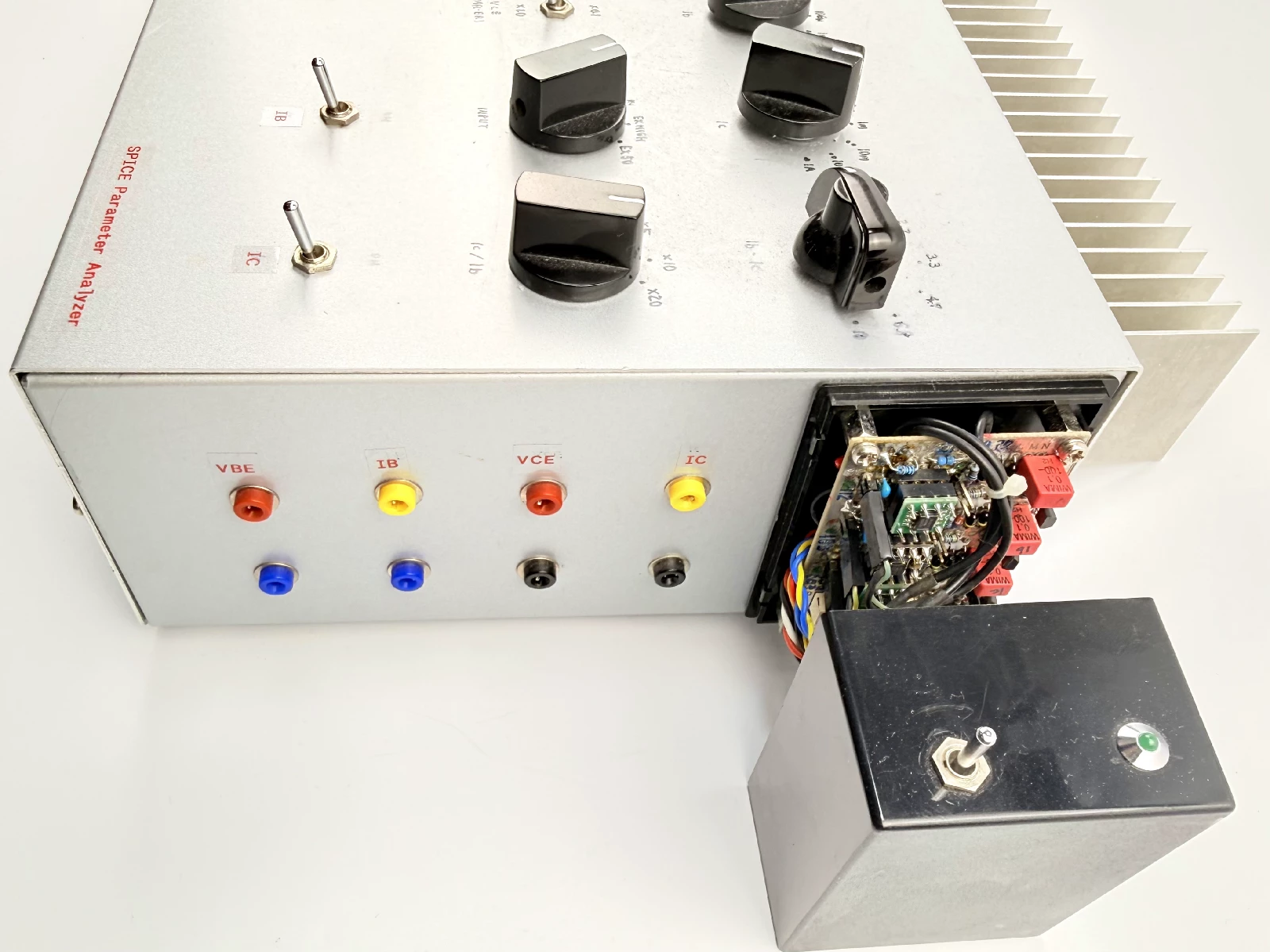
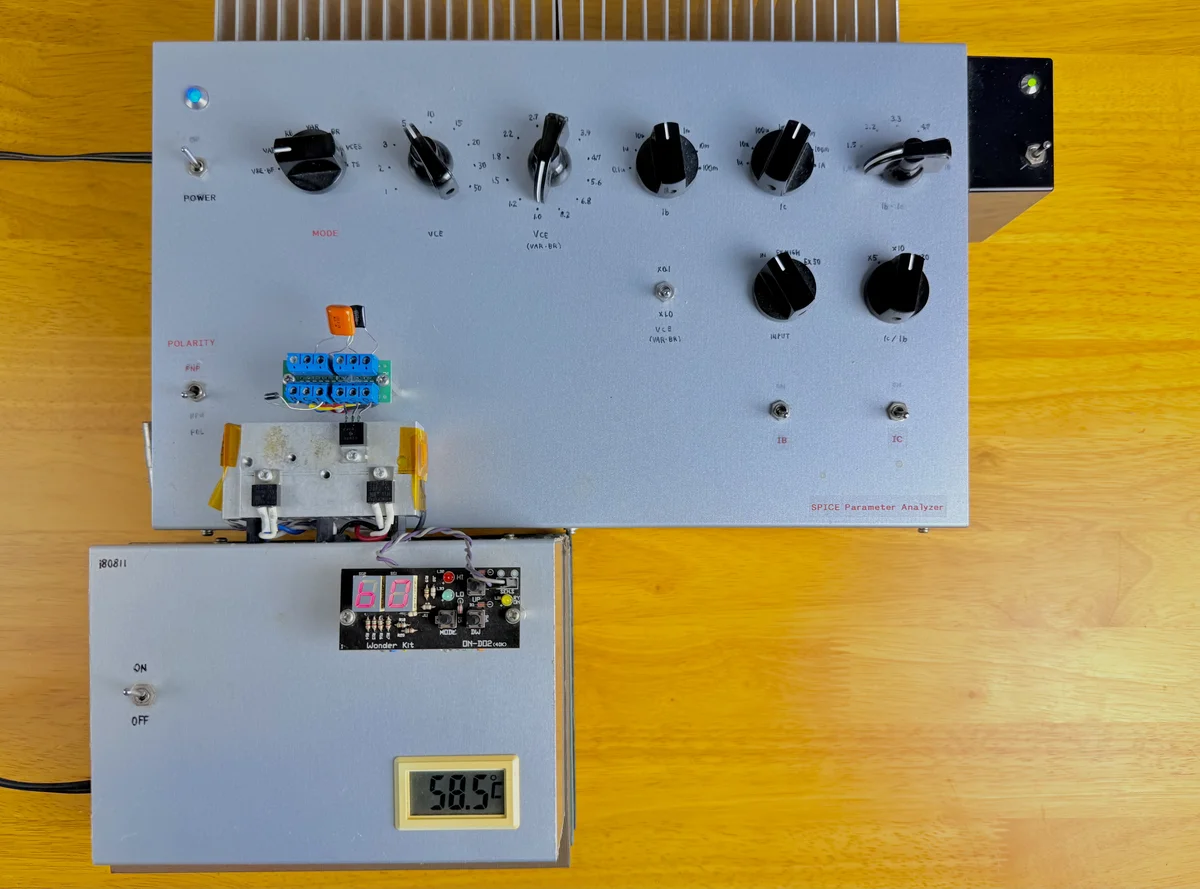
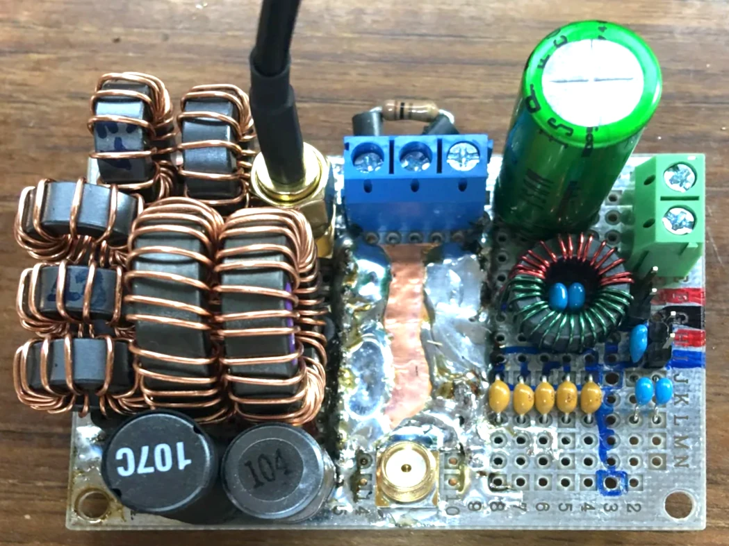
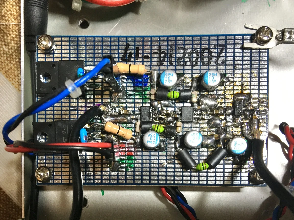
SPICE Parameter Analyzer
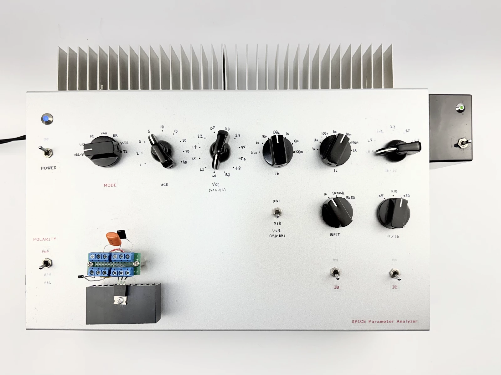
Almost all Gummel-Poon model parameters are extracted with this instrument, with the exception of the fT-related group and the Cob/Cib group.
The Agilent 33500B serves as the reference voltage source, controlling the range 1.000–10.000 V in both pulse and DC modes. Current and voltage measurement is shared across four DMMs.
| Function | Instrument | Notes |
|---|---|---|
| Reference voltage source | Agilent 33500B | Pulse & DC, 1.000–10.000 V |
| Current / voltage measurement (×4 ch) | HIOKI DT4282 × 2, Yokogawa TY-710, TY-720 | Simultaneous monitoring of Ib, Ic, Vce, Vbe |
| Waveform monitoring | Tektronix TBS1102B (100 MHz, 2 GS/s) | Pulse condition verification; Tstg measurement |
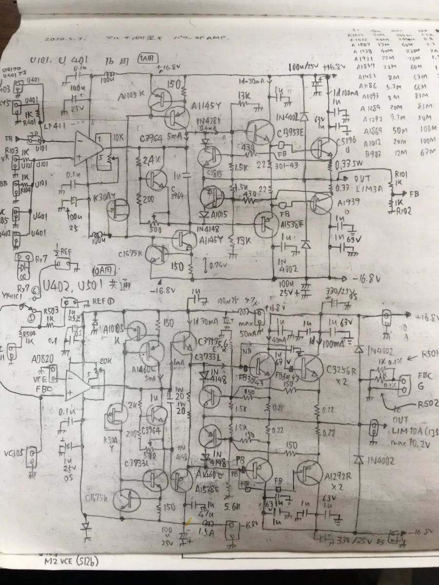
The instrument was completed in 2020. The details have grown hazy over time, but the layout and how it all works together — I built it myself, so the hands still remember. The handwritten notebook from the construction period is shown here. Circuit operating principles and component selection are documented in the SPICE Parameter Analyzer Circuit Detailed Notes.
All four DMMs fall in the high-resolution, high-accuracy class. The HIOKI DT4282 carries a DC basic accuracy of 0.025%; the Yokogawa TY-710/720, 0.03%. The difference between 60,000 counts (DT4282) and 50,000 counts (TY series) matters in the low-current region.
In fact, even for the DMMs, the early setup used more modest consumer-grade meters. But when pulse measurement began in earnest, the peak-hold function on general-purpose meters proved completely unable to capture pulse peaks.
That sent me poring through DMM catalogs until I settled on the Yokogawa TY-720 and the HIOKI DT4282. Neither publishes aperture jitter or effective sampling rate, but both appeared capable of capturing pulses around 250 µs, which was enough justification to buy.
In practice, the Yokogawa TY-720 turned out to hold its significant digits down to about 300 µs. The HIOKI DT4282 has a fast mode that captures shorter pulses than the TY-720, but the effective digit count drops to around two digits in that mode. Since all four meters do not need to operate at maximum speed simultaneously, this was accepted.
In the course of working through a thousand device types, however, overlay-structure high-frequency power transistors posed a major challenge. Whether because of their many small parallel cells, they retain heat readily — it turned out that pulse width had to be compressed to 30 µs or less to avoid self-heating errors affecting the results. This was confirmed using the HIOKI DT4282’s fast mode.
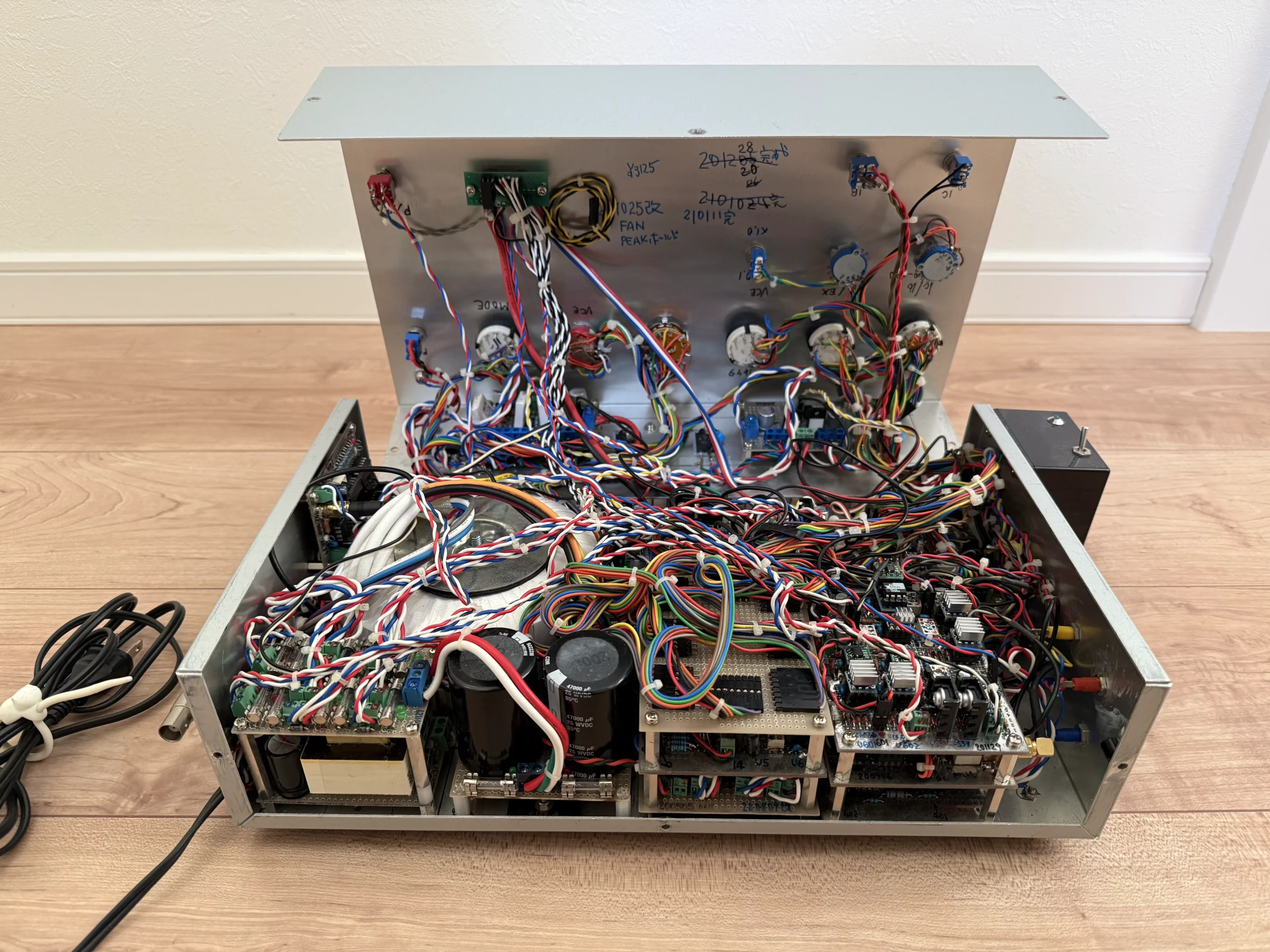
In the end, four high-speed, high-accuracy S/H circuits (for IB, IC, VBE, VCE) had to be built and added — six months after the original build was complete. There was no room inside the enclosure, so external mounting was the only option. The black box you see there is that add-on unit. There is an irony in having ended up with a system that no longer requires expensive DMMs. The minimum practical pulse width for this analyzer is approximately 30 µs.
Duty cycle during pulse measurement is set to 0.01% — the limit of the Agilent oscillator. The oscilloscope (Tektronix TBS1102B) monitors the waveform continuously, verifying that the pulse rise and fall are properly controlled and that no anomalies appear in the VBE and VCE waveforms.
Temperature-Controlled Heater Unit (for XTB Measurement)
hFE varies with temperature. XTB is the parameter in the Gummel-Poon model that captures this temperature dependence. It is not extracted automatically by the software; it must be calculated manually from hFE measurements at two temperatures.
The temperature-controlled heater unit was built for exactly this purpose. It holds the DUT at a stable temperature while hFE is measured, and XTB is calculated from the values obtained at two temperatures (25 °C and 60 °C).
The formula is straightforward.
T1 and T2 are expressed in absolute temperature (K): 25 °C → 298 K, 60 °C → 333 K. Measure hFE at both points and substitute.
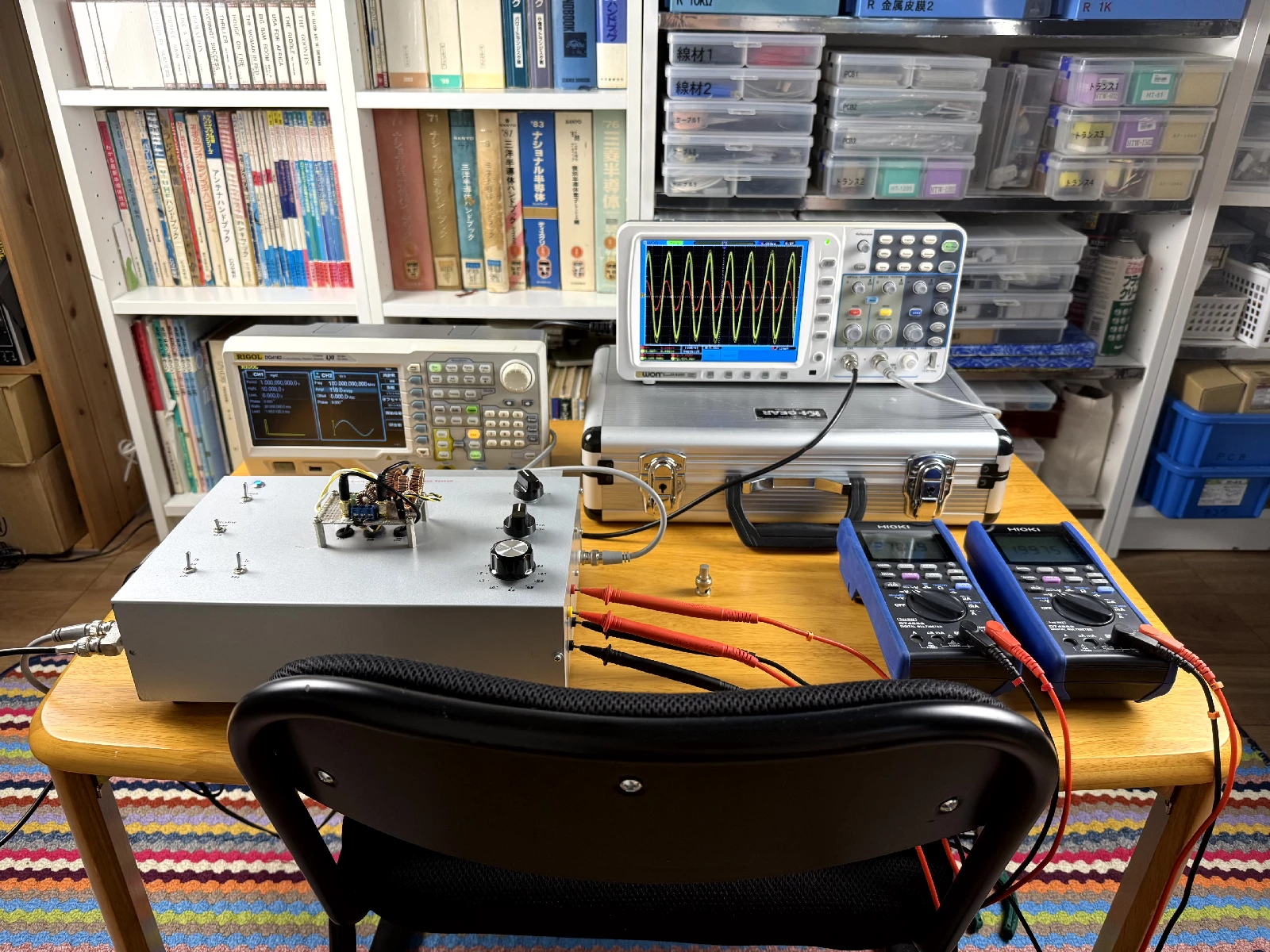
fT Measurement Fixture (130 MHz)
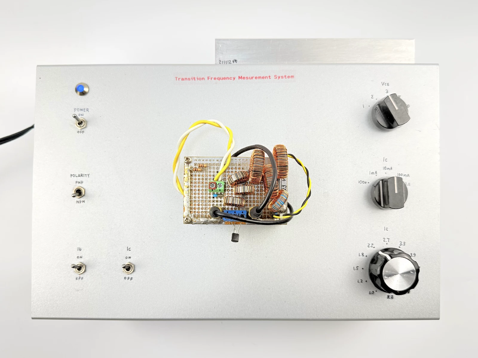
Used for the fT vs. Ic measurement. Extracts TF, ITF, XTF, and VTF.
The approach — keeping VCE constant while automatically controlling IB so that IC reaches the target value — is the same as in the SPICE parameter analyzer. The difference is the need to accurately detect the current waveform in the high-frequency domain.
| Function | Instrument | Notes |
|---|---|---|
| Sinusoidal signal source | Rigol DG4162 (160 MHz, 500 MSa/s) | Sine wave sweep around fT |
| Waveform observation | OWON DS8202 (200 MHz, 2 GSa/s) | Base and collector current waveforms |
The first challenge encountered during construction was base drive. The base input impedance (hie) changes with IC — high impedance at low IC, low impedance at high IC — making impedance matching meaningless as a concept. The countermeasure is to insert a high-value series resistor at the base to approximate constant-current drive, but this creates tradeoffs at high frequency. Too high a resistance produces an RC low-pass filter effect with associated loss; too low and the constant-current characteristic breaks down, increasing measurement error.
What makes this more troublesome is that this insertion point is itself a high-impedance node. Minor differences in implementation dramatically alter the measurement outcome. The solution that finally worked is to deliberately wire four tiny chip resistors in series, mounted by air-wiring. Using a single chip resistor fails at high frequency because the stray capacitance across the resistor’s terminals bypasses it, eliminating the resistive effect.
The choke coil for applying DC bias to the DUT presented the same challenge. By connecting multiple types and numbers of toroidal cores in series, the stray capacitance effect was minimized and high impedance maintained across the wide frequency range of 0.1–100 MHz. Trace lengths on the board were kept as short as possible to reduce inter-trace stray capacitance, while copper tape was used to create as large a ground plane as possible and stabilize the ground potential. This is also the fundamental reason the DUT mounting board was remade more than a dozen times.
The IC detection side also posed a formidable challenge. The voltage induced in the current transformer is extremely small — without at least 40 dB of amplification it is buried in noise and cannot be observed on the oscilloscope. Sweeping IC across two to three decades also demands wide dynamic range. Achieving full swing on a ±15 V supply, driving a 50 Ω load, and maintaining flat frequency response from 0.1 to 100 MHz — implementing all of this on a single board required a great deal of effort.
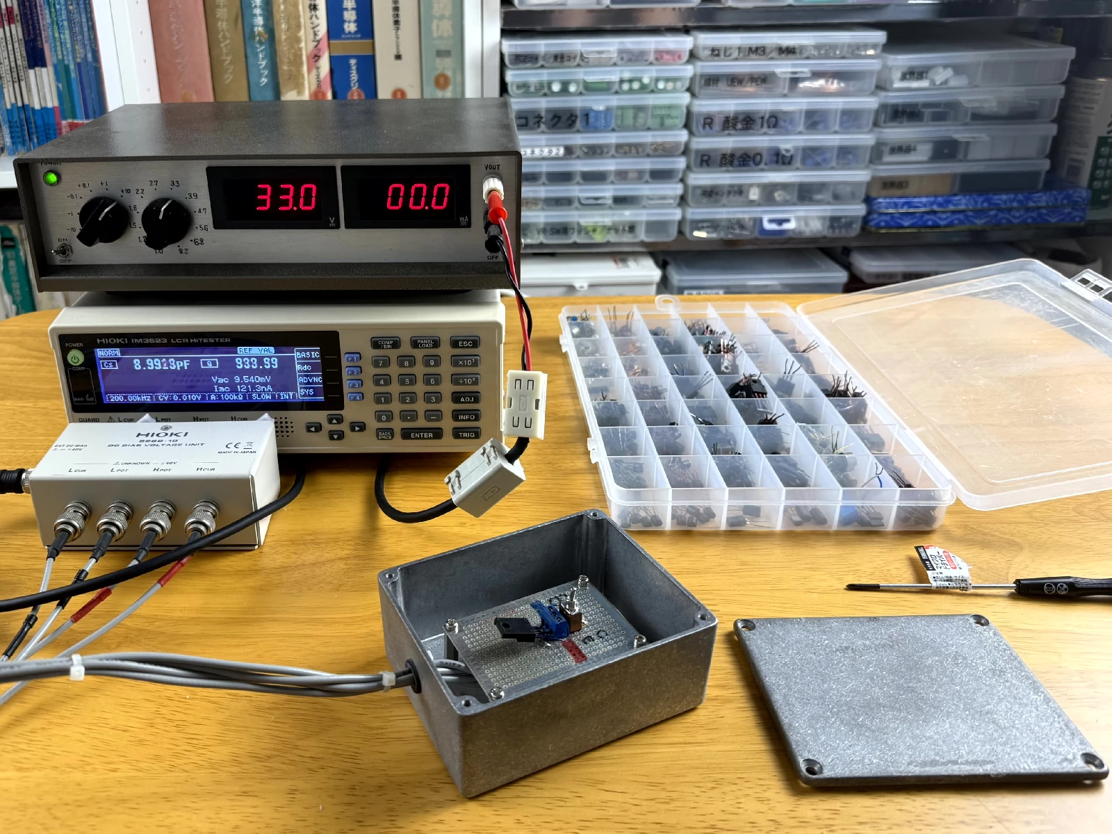
Cob/Cib Measurement System (DC Bias ±0.1–82.0 V)
The voltage dependence of junction capacitance is used to extract CJC, MJC, VJC, and FC (from Cob), and CJE, MJE, and VJE (from Cib).
| Function | Instrument | Notes |
|---|---|---|
| LCR meter | HIOKI IM3523 (40 Hz–200 kHz, ±0.05% rdg) | Direct junction capacitance measurement |
| DC bias supply | Custom-built (±0.1–82.0 V) | Installed inside shielded enclosure |
The HIOKI IM3523 carries an accuracy of ±0.05% rdg. Since Cob values are in the picofarad range, shielding against external noise and stray capacitance is essential. The bias supply circuitry is housed in a shielded enclosure for exactly this reason; omitting the shielding allows the readings to drift by tens of percent.
Building the capacitance meter was also considered initially, but the Lutron LCR-9183 — a cost-effective handheld unit — was found and used as the starting point. It reads to 0.01 pF with zero-compensation, and a maximum measurement frequency of 100 kHz is reasonable. A custom transistor socket board with integrated bias injection, connecting directly to the banana jacks, was also built.
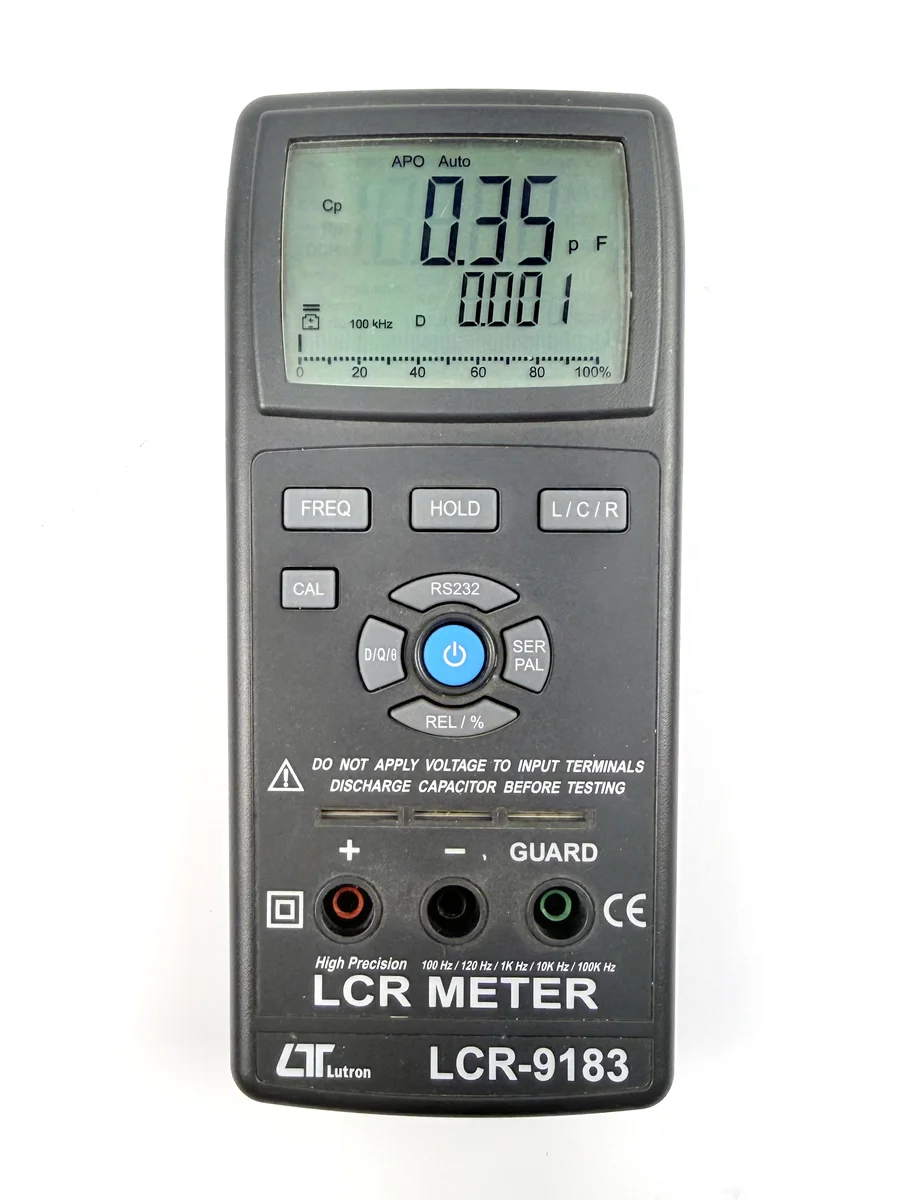
The problem lay in the low-voltage region of the Cbe measurement. To measure semiconductor capacitance, the junction must be held in a non-conducting state under reverse bias. When a sinusoidal measurement signal is superimposed, care must be taken not to violate the reverse-bias condition — silicon conducts at approximately 0.6 V, germanium at around 0.1 V. Some high-frequency germanium devices have a VEBO below 0.2 V; applying an incautious voltage carries a real risk of breakdown.
The LCR-9183 measures at 100 kHz. At that frequency, the base-emitter junction is fast enough to respond, so the measurement voltage must be kept to an absolute minimum — yet the LCR-9183’s test voltage exceeds 1 Vpp, and there is no way to adjust it. That was a dead end. It should be noted that measurement conditions in manufacturers’ datasheets typically specify 1 MHz. The higher frequency is presumably chosen to stay above the junction’s response speed, but a high-accuracy LCR meter capable of 1 MHz falls into a price range that is simply out of reach.
The switch was made to the HIOKI IM3523. It supports up to 200 kHz and allows the test voltage to be reduced to around 10 mV. Even high-frequency germanium devices with VEBO below 0.2 V can now be handled.
Even so, the battle against external noise continued. The lower the test voltage, the larger noise becomes in relative terms. By housing the bias supply circuitry in a shielded enclosure and combining that with the HIOKI IM3523’s averaging measurement function, the problem was finally contained.
A peculiar phenomenon also plagued the measurement for a long time. After applying bias voltage and reading capacitance on the LCR meter, the reading drifts gradually and eventually settles at a steady value — sometimes taking nearly five minutes per point. Initially this was suspected to be noise or a contact problem, but it was neither. That is simply how long it takes for the charge distribution within the junction to stabilize under the applied bias condition. Acquiring a complete Cob dataset from a single device can take close to an hour. This remains an unresolved issue today.
2-2 Digital Automation Is Not My Strength
As written on the About Kaz page, I am thoroughly hopeless at digital technology.
Connecting a microcontroller, a Raspberry Pi, or an Arduino via USB to transfer data automatically — that whole world is difficult for me. Designing a circuit, laying out a board, and soldering are no hardship; the moment software enters the picture, I stop cold. I learned electronics in the era when microcontrollers were still the cutting edge of the hobby. Assembling circuits from logic ICs and transistors, then chasing voltages with a multimeter — that was simply how things were done. Those habits have never left.
So all SPICE parameter measurements are done by hand.
Four DMMs lined up side by side — IB, IC, VCE, VBE read by eye. Written by hand on paper. hFE calculated with a pocket calculator as IC ÷ IB. hoe transferred first as raw IC–VCE data into Excel, computed there, then re-entered into the SPICE model extraction software. How much effort goes into finishing a single device — I have never counted, but it is formidable.
To be honest, I genuinely want to automate this. If I am being greedy — it would be ideal if the system entered the data into Micro-Cap for me. That vision has crossed my mind many times. But the prospect seems distant for now. There is also a promise to my wife to keep making progress on the site (About). Devices to measure are stacked up, there is LTspice to master, amplifiers to build, mysterious devices whose identity demands investigation — the list of things I want to do is so long that automation never quite reaches the top. I had at least considered building a division circuit to automate the hFE calculation alone. Then I discovered that analog multiplier ICs are apparently approaching end-of-life as well. Rather than getting closer to automation, I find myself worrying about parts availability. For now, I am leaving that lid quietly shut.
2-3 The Work Itself Becomes a Form of Error Detection
Manual measurement has unexpected strengths.
Because a human reads each result by eye at every measurement point, anomalous data are caught immediately — that is the core advantage.
The measurement workload per device is enormous. In a workflow where data are recorded blindly in bulk and then entered into the software afterwards, finding an anomalous point means remeasuring — by which time the ambient temperature may have shifted by a fraction of a degree. This is not a professional facility with a precision temperature-controlled chamber. Remeasuring a single point after an interval introduces the risk of ambient-temperature-related error on top of everything else.
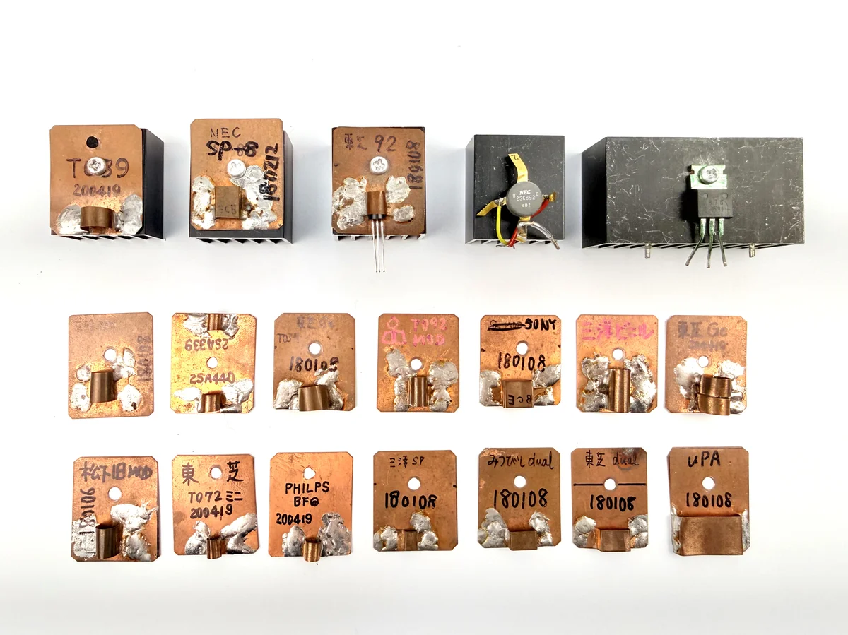
Countermeasures are in place against this. Air conditioning runs year-round to hold room temperature near 25 °C, and a circulator fan stirs the air to even out the temperature distribution. Each device is fitted with a heatsink through a custom-made copper adapter to minimize thermal influence as much as possible.
Even so, catching an anomalous reading mid-measurement and addressing it on the spot — versus discovering it in batch afterwards — produces a real difference in data reliability. In the sense that the effort itself functions as a detector, this approach carries genuine strength. Half sincere, half sour grapes, perhaps.
There is also an unexpected by-product. Measure one point, write the value on paper, punch the calculator for hFE, wait and remeasure if something looks off — by the time the next point is taken, ten seconds to nearly a minute has passed. This waiting time functions as a natural cooling interval. It ends up contributing to measurement accuracy and repeatability, so it is not entirely without merit.
2-4 What the Software Extracts, and What I Measure Myself
Micro-Cap Model 6.0.8 accepts measured data points across eight graphs and automatically fits the corresponding parameters. Not all parameters, however, are handled by the software.
Parameter extraction has a clear two-layer structure.
Layer 1: Parameters Extracted Automatically by the Software
Each graph and its corresponding primary parameters fall into this layer.
| Graph | Extracted Parameters |
|---|---|
| Vbe vs Ic | RE, NF, IS |
| Beta vs Ic | NE, ISE, BF, IKF |
| hoe vs Ic | VAF |
| Vce(sat) vs Ic | RC, NC, ISC, IKR |
| Ic vs Tstg | TR |
| Cob vs Vcb | CJC, MJC, VJC, FC |
| Cib vs Veb | CJE, MJE, VJE |
| fT vs Ic | TF, ITF, XTF, VTF |
Layer 2: Parameters Measured Manually and Entered by Hand
Some parameters do not appear on the software’s control panels — they are outside the scope of automatic extraction and must be measured independently by the experimenter and entered manually.
| Parameter | Description | Measurement Method |
|---|---|---|
| VAR | Reverse Early voltage | Calculated from reverse hoe measurement |
| BR | Reverse current gain | Measured with emitter and collector reversed |
| XTB | Temperature coefficient of hFE | Measured at two temperatures (25 °C / 60 °C) using the custom temperature-controlled heater |
| RB | Base resistance | Calculated from Vbe characteristics at high current |
| RBM | Minimum base resistance | Same as above |
| IRB | Current at which RB transitions to RBM | Same as above |
The parts the software cannot handle must be measured and filled in by a human before the model is complete. This two-layer structure is what “full-parameter measurement” actually means.
2-5 Where DC Measurement Has the Advantage
The SPICE parameter analyzer does not measure everything by pulse.
In the region below Ic = 100 µA, DC measurement is used.
The reason: at the instant a pulse is applied, the charging current into the base-emitter junction capacitance Cje superimposes on the base current. In the low-Ic region, this transient current is too large to ignore. Even with a pulse width of 1 ms, the time required for Cje to charge fully leaves a residual measurement error.
With DC measurement, steady-state conditions are guaranteed. The thermal issue is contained because Ic is small enough that self-heating stays within a negligible range. For the 2SC1815 at IC = 100 µA and VCE = 5 V, the dissipated power is 0.5 mW — the junction temperature rise from self-heating is less than 1 °C.
This switchover point varies by device. A larger Cje means more time to charge, shifting the transition point toward higher currents. The 2SC1815 has a small Cje in absolute terms (measured at 14.686 pF), so 100 µA is fine.
Chapter 3 What the Measurements Revealed
3-1 Results
The measured SPICE parameters for the 2SC1815-Y (TO-92, Toshiba, NPN) are given below. Device measured: one individual specimen. Measurement temperature: 24.6 °C.
Published Models vs. Kaz Measured Models (All Ranks) — Comparison Table
| Parameter | 2SC2712 Toshiba Official |
2SC1815 MC5CQ |
2SC1815-O Kaz Measured |
2SC1815-Y Kaz Measured |
2SC1815-GR Kaz Measured |
2SC1815-BL Kaz Measured |
|---|---|---|---|---|---|---|
| IS | 40f | 271.38f | 9.111f | 9.097f | 16.045f | 30.011f |
| BF | 160 | 196 | 118.821 | 173.744 | 275.022 | 454.489 |
| NF | 1 | — | 0.99959 | 0.99634 | 0.99569 | 0.99721 |
| VAF | 30 | 372.6 | 757.064 | 400.547 | 526.372 | 147.783 |
| IKF | 0.3 | 0.14886 | 0.624 | 0.558 | 0.293 | 0.229 |
| ISE | 50f | 2.2915p | 683.734f | 51.624f | 157.886f | 100.006f |
| NE | 1.5 | — | 1.7226 | 1.66209 | 1.62711 | 1.6551 |
| BR | 5 | 0.167 | 8.538 | 4.519 | 4.268 | 6.004 |
| VAR* | 1000 | — | 76 | 76 | 88 | 60 |
| IKR | 0.001 | — | 0.030 | 0.030 | 0.056 | 0.056 |
| ISC | 100f | — | 8.791p | 92.629p | 57.614p | 8.417p |
| NC | 1 | — | 1.5 | 1.8 | 1.8 | 1.600 |
| RE | 0.001 | — | 0.721 | 0.539 | 0.546 | 0.523 |
| RB | 10 | 40 | 64 | 16 | 34 | 44 |
| RBM | — | — | 1.000 | 0.680 | 0.380 | 1.300 |
| IRB | — | — | 0.0014 | 0.002 | 0.0029 | 0.0023 |
| RC | 0.3 | 0.72 | 0.177 | 0.254 | 0.332 | 0.279 |
| CJE | 10p | 4.717p | 18.444p | 14.686p | 11.936p | 12.036p |
| VJE | 0.75 | — | 0.615 | 0.622 | 0.637 | 0.591 |
| MJE | 0.33 | — | 0.317 | 0.315 | 0.328 | 0.310 |
| CJC | 5p | 4.8153p | 5.676p | 5.387p | 5.046p | 5.456p |
| VJC | 0.75 | — | 0.400 | 0.393 | 0.408 | 0.395 |
| MJC | 0.33 | — | 0.282 | 0.275 | 0.302 | 0.277 |
| FC | 0.5 | — | 0.940 | 0.900 | 0.920 | 0.890 |
| TF | 250p | 993p | 737.235p | 609.854p | 451.405p | 426.909p |
| XTF | 30 | — | 0.470 | 1.100 | 3.000 | 1.800 |
| VTF | 2 | — | 2.5 | 2.5 | 2.5 | 2.5 |
| ITF | 0.2 | — | 0.195 | 0.166 | 0.134 | 0.172 |
| TR | 40n | — | 872.251n | 1.104u | 919.518n | 604.231n |
| XTB | 2 | — | 1.5 | 1.7 | 1.9 | 1.6 |
| T_MEASURED ‡ | 25 | — | 25.5 | 23.7 | 26.6 | 24.6 |
*VAR: A parameter not displayed on the Micro-Cap Model 6.0.8 control panel; confirmed by inspecting the LIB file directly. Not all parameters listed here are presented with full confidence. In particular, RB, RBM, IRB, ISC, ISE, TR, and FC are still under verification. Distribution of the parameter set will be made once multi-lot validation is complete.
‡ T_MEASURED: Ambient room temperature (°C) during measurement for each rank. Not a SPICE parameter; included as reference.
Model Listing for LTspice
; 2SC1815 Kaz-electro measured models  2022.03
; https://kaz-electro.jp

.MODEL 2SC1815-O NPN (
+ IS=9.111F BF=118.821 NF=0.99959 VAF=757.064
+ IKF=0.624 ISE=683.734F NE=1.7226 BR=8.538
+ VAR=76 IKR=0.030 ISC=8.791P NC=1.5
+ RE=0.721 RB=64 RBM=1.000 IRB=0.0014 RC=0.177
+ CJE=18.444P VJE=0.615 MJE=0.317
+ CJC=5.676P VJC=0.400 MJC=0.282 FC=0.940
+ TF=737.235P XTF=0.470 VTF=2.5 ITF=0.195
+ TR=872.251N XTB=1.5)

.MODEL 2SC1815-Y NPN (
+ IS=9.097F BF=173.744 NF=0.99634 VAF=400.547
+ IKF=0.558 ISE=51.624F NE=1.66209 BR=4.519
+ VAR=76 IKR=0.030 ISC=92.629P NC=1.8
+ RE=0.539 RB=16 RBM=0.680 IRB=0.002 RC=0.254
+ CJE=14.686P VJE=0.622 MJE=0.315
+ CJC=5.387P VJC=0.393 MJC=0.275 FC=0.900
+ TF=609.854P XTF=1.100 VTF=2.5 ITF=0.166
+ TR=1.104U XTB=1.7)

.MODEL 2SC1815-GR NPN (
+ IS=16.045F BF=275.022 NF=0.99569 VAF=526.372
+ IKF=0.293 ISE=157.886F NE=1.62711 BR=4.268
+ VAR=88 IKR=0.056 ISC=57.614P NC=1.8
+ RE=0.546 RB=34 RBM=0.380 IRB=0.0029 RC=0.332
+ CJE=11.936P VJE=0.637 MJE=0.328
+ CJC=5.046P VJC=0.408 MJC=0.302 FC=0.920
+ TF=451.405P XTF=3.000 VTF=2.5 ITF=0.134
+ TR=919.518N XTB=1.9)

.MODEL 2SC1815-BL NPN (
+ IS=30.011F BF=454.489 NF=0.99721 VAF=147.783
+ IKF=0.229 ISE=100.006F NE=1.6551 BR=6.004
+ VAR=60 IKR=0.056 ISC=8.417P NC=1.600
+ RE=0.523 RB=44 RBM=1.300 IRB=0.0023 RC=0.279
+ CJE=12.036P VJE=0.591 MJE=0.310
+ CJC=5.456P VJC=0.395 MJC=0.277 FC=0.890
+ TF=426.909P XTF=1.800 VTF=2.5 ITF=0.172
+ TR=604.231N XTB=1.6)
3-2 On Fit Error
Micro-Cap Model 6.0.8 displays the fit error between measured points and model curves as a percentage. Interpreting this error correctly is important for judging the reliability of a measurement.
The fit errors for each graph of the 2SC1815-Y are shown below.
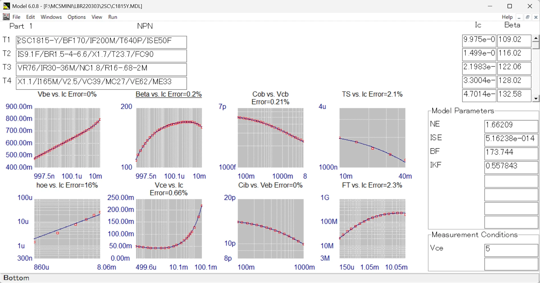
| Graph | Databook Readings (Sec. 1-1) | Kaz Full-Parameter Measurement (Sec. 3-1) |
|---|---|---|
| Vbe vs Ic | 0.82% | 0% |
| Beta vs Ic | 9.2% | 0.2% |
| hoe vs Ic | 7% | 16% |
| Vce(sat) vs Ic | 2.9% | 0.66% |
| Cob vs Vcb | 1.1% | 0.21% |
| Cib vs Veb | 0.15% | 0% |
| fT vs Ic | 15% | 2.3% |
| Tstg vs Ic | 0% | 2.1% |
After re-entering all parameters from direct measurement, Beta vs. Ic improved from 9.2% to 0.2%, and fT vs. Ic from 15% to 2.3%. Supplying a sufficient number of carefully collected data points can bring fit error below 1%, and in some cases to 0%. This is the payoff of extracting all parameters from a single device.
On the other hand, hoe vs. Ic moved in the wrong direction, from 7% to 16%. This relates to the extraction accuracy of VAF — the Early voltage. The fact is noted here; a full discussion is deferred to another occasion.
A low fit error means the model reproduces the measured values well. That does not, however, make a low-error model correct. A current-dependent parameter such as XTF is highly sensitive to the density and range of measurement points — the fit result can change dramatically depending on how the data are collected. A model with 0% error gives no guarantee of accurately predicting behavior outside the measured range.
Chapter 4 Discussion and What Comes Next
4-1 What Changes Across Ranks?
As the measurements accumulate, a question arises. With each step up the rank ladder, it is not only BF that appears to shift — IS and TF seem to move in concert. Is that just an impression?
To find out, the parameters for all four ranks — O, Y, GR, and BL — were normalized to Y as unity (1.0) and plotted.
Y (Yellow / Reference = 1.0)
GR (Green)
BL (Blue)
Measured values (Kaz, 2022.03): O: BF=118.821, IKF=0.624, TF=737.235p, IS=9.111f, CJE=18.444p / Y: BF=173.744, IKF=0.558, TF=609.854p, IS=9.097f, CJE=14.686p / GR: BF=275.022, IKF=0.293, TF=451.405p, IS=16.045f, CJE=11.936p / BL: BF=454.489, IKF=0.229, TF=426.909p, IS=30.011f, CJE=12.036p
The result was clear. BF increases monotonically from O through BL — O: 0.68×, Y: 1.0×, GR: 1.58×, BL: 2.62×. IKF and TF, however, move in the opposite direction. IKF decreases from O: 1.12× to BL: 0.41×; TF from O: 1.21× to BL: 0.70×. IS jumps to 3.30× at BL.
The physical interpretation is straightforward. Rank sorting is essentially a classification of base-thickness variation. The diffusion process can target a base thickness, but temperature non-uniformity across the wafer and variability in diffusion time are unavoidable. A thinner-than-nominal die delivers higher hFE — BF rises. At the same time, carriers traverse a thin base more easily, shortening the transit time TF. High-injection effects also set in earlier, reducing IKF. Improved minority-carrier injection efficiency raises IS. The rank difference is a consequence of a single physical quantity — base thickness — expressing itself simultaneously across multiple parameters.
In other words, it is not only BF that changes. BF and IKF, TF, and IS are linked indirectly through a shared physical origin.
This fact also suggests a limitation of parametric analysis. Varying only BF brings the mid-current hFE characteristic into alignment, but the high-current behavior (IKF), high-frequency characteristics (TF, CJE), and low-current leakage (IS) remain unaccounted for. Parameters measured individually from a single device form a self-consistent set — not nominal values, not statistical medians, but internally coherent numbers extracted from one specimen. That coherence is the foundation of simulation accuracy.
BR also tends to be overlooked. This is probably because operating the device with C-E reversed is rare except for special applications such as muting circuits. Yet BR directly affects saturation-region behavior — VCE(sat) — and can be significant in switching-circuit simulation. BR is not extracted by the software’s automatic fitting; it is obtained from a measurement taken with emitter and collector reversed.
This is one of the reasons I fell into the pursuit of measuring a thousand device types. Curiosity was ignited.
4-2 Lot and Generation Differences
The parameters published here are measured values from a specific lot and a specific individual specimen. Even two 2SC1815-Y parts from different production eras may need to be treated as different devices. Over the more than thirty years of production — from the 1976 introduction through the 2012–2013 end-of-life — it cannot be claimed with certainty that the fabrication process remained unchanged throughout. This question will be addressed in a separate article (2SA1015 / 2SC1815 — Japan’s Most Famous Complementary Pair).
4-3 Closing Remarks
This report used the 2SC1815 as a worked example to give an informal account of the SPICE parameter modeling activities on this site — covering methodology and equipment — and to share the results.
Comparison against the official model (2SC2712) and the MC5CQ bundled model confirmed discrepancies across many parameters. The causes of those differences will be examined in a follow-up discussion after the 2SC2712 itself has been measured.
The next task is to verify lot and generation differences. Results will be published as the work progresses.